First, the challenge posed by Hawking
It is often stated that Stephen Hawking once pointed out two fundamental problems faced by semiconductor manufacturers:
(1) The finite speed of light
(2) The atomic nature of matter
The first issue is that within one CPU cycle, an electrical signal cannot reach every CPU in the entire system. For instance, when CPU0 executes the instruction "foo = 1" on the global variable foo, after CPU0 finishes executing the corresponding assembly code, other CPU cores may still see the previous value of foo. Those new to operating systems should take note of this.
The second issue arises because we need at least one atom to store binary bits. It's impossible to store a word, a section of memory, or the contents of an entire register in a single atom... The end result is that hardware engineers cannot indefinitely reduce the chip area. As the number of CPU cores increases, the burden of inter-core communication grows heavier.
Of course, as a theoretical physicist, Hawking’s concerns are theoretical. It’s quite possible that semiconductor manufacturers are nearing these two limits. Nevertheless, there are ongoing R&D efforts focused on finding ways to circumvent these two fundamental limitations.
One way to overcome the atomic nature of matter involves using a material known as a "high-k insulator," which allows larger devices to mimic the electrical properties of ultra-small devices. While this material presents significant production challenges, it could eventually push the boundaries of research further. Another potential solution is storing multiple bits on a single electron, based on the principle that a single electron can exist at multiple levels simultaneously. However, this approach remains unproven and needs to be tested to determine whether it can work reliably in commercial-grade semiconductor devices.
There is also a solution called "quantum dots," which could enable the creation of much smaller semiconductor devices, though the method is still in the research phase.
The first limitation is difficult to bypass, although quantum technology, and even string theory, theoretically allow communication speeds to exceed the speed of light. But this is purely theoretical research and has yet to find practical application in engineering.
Secondly, how slow are atomic operations?
By "atomic operations," I mean those like the Linux kernel's atomic_long_add_return API. To put it simply, when an atomic operation is completed, all CPU cores must recognize the changes made to the atomic variables, and no other CPU cores should modify these variables during the atomic operation. This inevitably requires broadcasting the corresponding electrical signal between all CPUs.
For regular variable operations (non-atomic operations), the electrical signal does not have to propagate between all CPU cores and go back and forth:
Keep in mind that the Linux operating system can run on large systems with over 1024 CPUs. In these massive systems, it takes a "long" time to broadcast an electrical signal between all CPUs.
But how long exactly is this time?
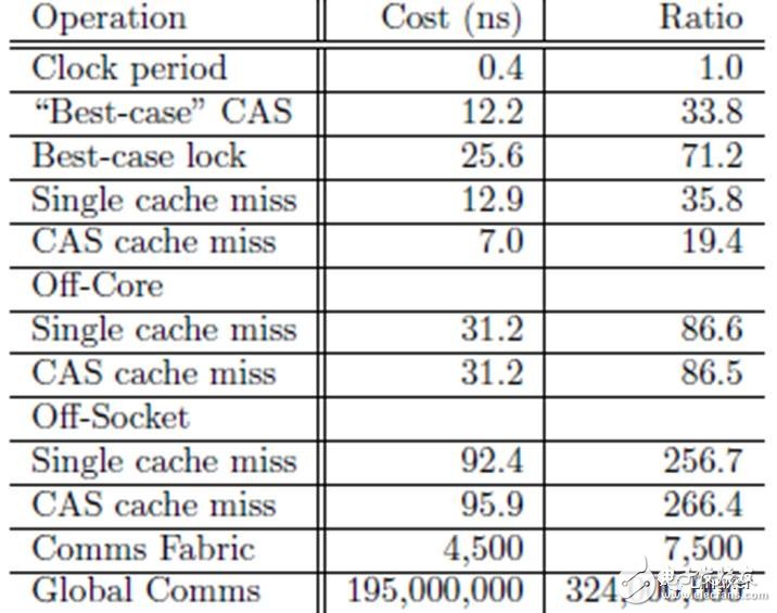
In the above table, the CPU cycle for a "CAS cache miss" is 266. Is this long enough? And this test result was conducted on a relatively new multicore system with 4-core CPUs. In older systems, or in systems with more CPU cores, this would be even longer.
Thirdly, variables can have multiple values
This isn’t just a fantasy.
Assume that CPU 0 writes a value of 1 to the global variable foo. We naturally think that other CPUs will immediately recognize that foo now has a value of 1. Even if we have doubts, we might take a step back and think that at some later time, all other CPUs will simultaneously recognize that foo has a value of 1. Unfortunately, this idea must be abandoned. Parallel computing is magical and counterintuitive. Without understanding this concept, there’s no way to truly grasp RCU (Read-Copy-Update).
To understand this, consider the following code snippet. It is executed in parallel by several CPUs. The first line sets the value of the shared variable to the current CPU ID, and the second line calls the gettb() function to initialize several values. This function reads the hardware time count, which is provided by the SOC hardware and shared between all CPUs. Of course, this hardware count is primarily valid on the Power architecture, and I often use it on the PowerPC e500 architecture. The loop in lines 3-8 records the duration during which the variable is held on the current CPU.
1 state.variable = mycpu;
2 lasttb = oldtb = firsttb = gettb();
3 while (state.variable == mycpu) {
4 lasttb = oldtb;
5 oldtb = gettb();
6 if (lasttb - firsttb > 1000)
7 break;
8 }
Before exiting the loop, firsttb will save a timestamp, which is the time of the assignment. Lasttb also holds a timestamp, which is the sampled value of the last value assigned to the shared variable. If the shared variable has changed before entering the loop, it is equal to firsttb.
This data was collected on a 1.5GHz POWER5 8-core system. Each core contains a pair of hardware threads. CPUs 1, 2, 3, and 4 record values, while CPU 0 controls the test. The timestamp counter period is 5.32ns, which is sufficient for us to observe the cache status.
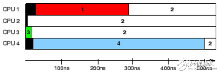
The results in the above figure show the time each CPU recognizes that the variable is held. Each horizontal bar indicates the time at which the CPU observed the variable, and the black area on the left indicates the time the corresponding CPU first counted. During the first 5ns, only CPU 3 has the value of the variable. At the next 10ns, CPUs 2 and 3 see inconsistent variable values, but then all agree that their value is "2". However, CPU 1 considers its value to be "1" for the entire 300ns, and CPU 4 considers its value to be "4" for the entire 500ns.
This is truly an incredible test result. The same variable shows different values on different CPUs!
If you don’t understand the hardware, you won’t accept this incredible test result. Of course, if there were a master standing in front of you at this moment, you couldn’t dance to their rhythm.
Fourth, why MESI?
Please don’t say: I don’t know what MESI is?
In short, MESI is a memory cache coherence protocol.
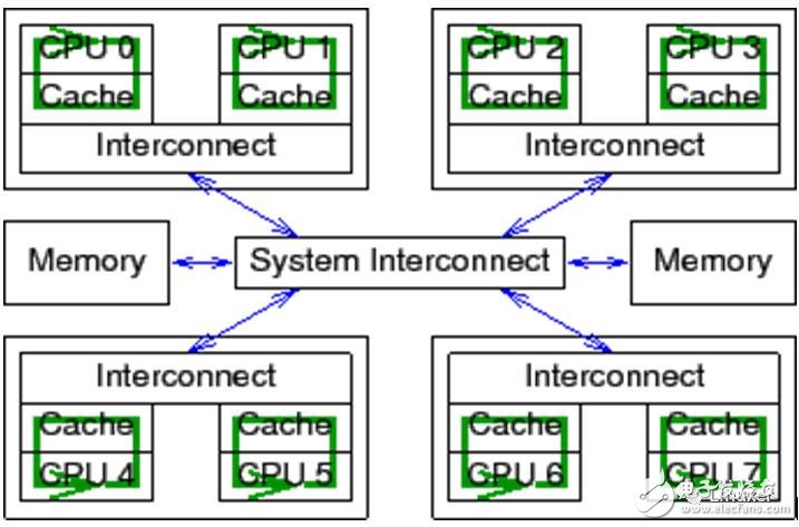
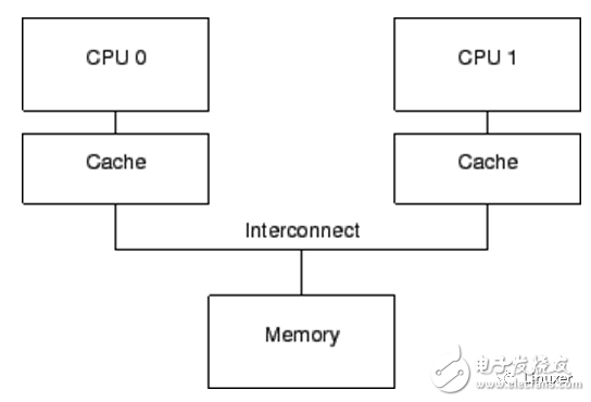
Modern CPUs are much faster than modern memory systems. In 2006, a CPU could execute ten instructions per nanosecond. But it takes many tens of nanoseconds to retrieve a piece of data from physical memory. Their speed difference (over two orders of magnitude) has led to the emergence of several megabytes of cache in modern CPUs. These caches are closely tied to the CPU, as shown below. Typically, the cache can be accessed in a few clock cycles. With the help of the CPU pipeline, we can assume that the cache can offset the impact of memory on CPU performance.
The data stream between the CPU cache and the memory is a fixed-length block called a "cache line," which is typically 2^N bytes in size. The range varies from 16 to 256 bytes. When a specific piece of data is accessed by the CPU for the first time, it does not exist in the cache. This is called a "cache miss" (or more accurately, "startup cache miss" or "warmup cache miss"). A "cache miss" means that when the CPU reads data from physical memory, it must wait (or "stall") for hundreds of CPU cycles. However, after the data is loaded into the CPU cache, subsequent accesses will be found in the cache, allowing the CPU to run at full speed.
After a period of time, the CPU’s cache will fill up, and subsequent cache misses will require swapping out existing data in the cache to make room for the most recently accessed data. This "cache miss" is called a "capacity miss" because it is caused by cache capacity limitations. However, even if the cache is not full at this point, a large amount of cache may be swapped out due to a new data access. This is because large amounts of cache are implemented using hardware hash tables. These hash tables have fixed-length hash buckets (or "sets," which CPU designers call them), as shown in the following figure.
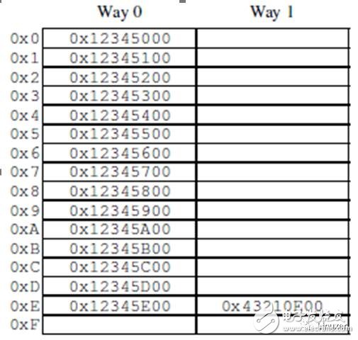
This cache has 16 "sets" and 2 "ways," for a total of 32 "cache lines." Each node contains a 256-byte "cache line," which is a 256-byte aligned block of memory. This cache line is slightly larger, but it makes hexadecimal operations easier. From a hardware perspective, this is a two-way set associative cache, similar to a software hash table with 16 buckets, each with a hash chain of up to two elements. The size (32 cache lines in this case) and the connectivity (2 in this case) are called the cache's "geometry." Since the cache is implemented in hardware, the hash function is very simple: take 4 bits (the number of hash buckets) from the memory address as a hash key.
The situation depicted in the figure may occur when the program code is at address 0x43210E00-0x43210EFF and the program accesses the address 0x12345000-0x12345EFF in sequence. Assuming the program is about to access address 0x12345F00, this address will be hashed to line 0xF. Both lines of the line are empty, so the corresponding 256-byte cache line can be provided. If the program accesses address 0x1233000, it will hash to line 0, and the corresponding 256-byte cache line can be placed on the 1st way. However, if the program accesses address 0x1233E00, it will hash to line 0xE, and a cache line must be replaced to make room for the new line. If you subsequently access the replaced line, a "cache miss" will be generated, and such a cache miss is called an "associativity miss."
Furthermore, we only considered the case of reading data. What happens when I write? It is important to ensure that all CPUs are aware that the data has been modified before writing data to a particular CPU. Therefore, it must first be removed from other CPU caches, or "invalidated." Once the "invalidate" operation is completed, the CPU can safely modify the data item. If the data exists in the CPU cache but is read-only, this process is called a "write miss." Once a particular CPU has caused other CPUs to complete the "invalidate" operation, the CPU can repeatedly rewrite (or read) the data.
Finally, if another CPU attempts to access the data item, it will cause a cache miss. At this time, because the first CPU invalidated the cache entry for writing, this is called a "communication miss." This usually occurs when several CPUs use cache communication (for example, a lock for a mutex algorithm uses this data item to communicate between CPUs).
Obviously, all CPUs must be careful to maintain a consistent view of the data. These problems are prevented by the "cache coherence protocol," which is MESI.
Fifth, the four states of MESI
MESI has four states: "modified," "exclusive," "shared," and "invalid." The protocol can apply these four states to a specified cache line. Therefore, the protocol maintains a two-bit status tag in each cache line, which is appended to the physical address and data of the cache line.
A cache line in the "modified" state is due to the recent memory storage of the corresponding CPU. And the corresponding memory ensures that it does not appear in the cache of other CPUs. Therefore, the cache line in the "modified" state can be considered "owned" by the CPU. Since the cache holds the "latest" data, the cache is ultimately responsible for writing data back to memory, and should provide data for other caches, and must do so before caching other data.
The "exclusive" state is very similar to the "modified" state. The only difference is that the cache line has not been modified by the corresponding CPU. This also means that the data in the cache line and the data in the memory are up to date. However, since the CPU can store data to the line at any time regardless of other CPUs, the "exclusive" state can also be considered "owned" by the corresponding CPU. That is, since the value in physical memory is up to date, the line can be discarded directly without writing back to memory, and there is no need to notify other CPUs.
Cache lines in the "shared" state may have been copied to the cache of at least one other CPU so that data cannot be stored to the cache line without the permission of other CPUs. The same as the "exclusive" state, the value in the memory is the latest, so you can directly discard the value in the cache without writing back the value to the memory, and do not need to notify other CPUs.
The line in the "invalid" state is empty, in other words, it does not hold any valid data. When new data enters the cache, it is placed into a cache line that is in the "invalid" state. This method is better because replacing cached lines in other states will cause a lot of cache misses.
Since all CPUs must maintain a data consistency view in the cache line, the cache coherency protocol provides messages to identify the actions of cache lines in the system.
Sixth, MESI news
The MESI protocol requires communication between CPUs. If the CPU is on a single shared bus, only the following messages are sufficient:
Read message: The "read" message contains the physical address of the cache line to be read.
Read Response Message: The "Read Response" message contains data for the earlier "read" message. This "read response" message may be provided by physical memory or by a cache of other CPUs. For example, if a cache is in the "modified" state, its cache must provide a "read response" message.
Invalid message: The "make invalid" message contains the physical address of the cache line to invalidate. Other caches must remove the corresponding data from their cache and respond to this message.
Invalid acknowledgment: A CPU that receives an "make invalid" message must respond to an "make invalid reply" message after removing the specified data.
Invalid read: The "read invalid" message contains the physical address to be read by the cache line. It also instructs other caches to remove data. Therefore, it contains both a "read" message and an "invalid" message. The "read invalid" message requires both a "read response" message and an "make invalid reply" message.
Write back: The "write back" message contains the address and data to be written back to physical memory. (and may "probe" the cache of other CPUs). This message allows the cache to swap out data in the "modified" state when necessary to make room.
Again, all of these messages require the propagation of electrical signals between CPUs, both of which face the two IT challenges that Hawking proposed.
Seventh, MESI state transitions
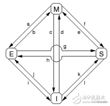
Transition (a): The cache line is written back to physical memory, but the CPU still keeps it in the cache and modifies it later. This conversion requires a "write back" message.
Transition (b): The CPU writes data to the cache line, which is currently in exclusive access. No need to send or receive any messages.
Transition (c): The CPU receives a "read invalid" message and the corresponding cache line has been modified. The CPU must invalidate the local copy and then respond to the "read response" and "make invalid reply" messages while sending data to the requesting CPU, indicating that its local copy is no longer valid.
Transition (d): The CPU performs an atomic read-modify-write operation with the corresponding data not in its cache. It sends a "read invalid" message and receives the data via a "read response" message. Once it receives a complete "make invalid response" response set, the CPU completes the conversion.
Transition (e): The CPU performs an atomic read-modify-write operation, and the corresponding data is read-only in the cache. It must send an "make invalid" message and wait for the "make invalid reply" response set to complete the conversion.
Transition (f): Some other CPUs read the cache line, the data is provided by the CPU, and the CPU contains a read-only copy. The reason for the read-only data may be because the data has been written back into memory. This conversion begins with the receipt of a "read" message, and eventually the CPU responds with a "read response" message.
Transition (g): Other CPUs read data and the data is provided from the cache or physical memory of the CPU. In either case, the CPU retains a read-only copy. The transaction begins with receiving a "read" message, and eventually the CPU responds with a "read response" message.
Transition (h): The current CPU will soon write some data to the cache line, so an "invalid" message is sent. The CPU does not complete the conversion until it receives all the "Invalid Reply" messages. Optionally, all other CPUs swap out the data of the cache line by "writing back" messages (possibly making room for other cache lines). Thus, the current CPU is the last CPU that cached this data.
Transition (i): Some other CPUs have performed an atomic read-modify-write operation, and the corresponding cache line is only held by the CPU. This CPU turns the cache line into an invalid state. This conversion begins with the receipt of a "read invalid" message, and eventually the CPU responds with a "read response" message and an "make invalid reply" message.
Transition (j): This CPU saves a data to the cache line, but the data is not yet in its cache line. Therefore, a "read invalid" message is sent. The transaction is not completed until it receives a "read response" message and all "make invalid responses" messages. Cache lines may transition to the "modified" state very quickly, which is done by Transition (b) after the storage is complete.
Transition (k): This CPU loads one data, but the data is not yet in the cache line. The CPU sends a "read" message and completes the conversion when it receives the corresponding "read response" message.
Transition (l): Other CPUs store a single row of data to the cache line, but the cache line is read-only (because other CPUs also hold the cache line). This conversion begins with the receipt of an "Invalid" message, and the current CPU eventually responds with an "Invalid Reply" message.
This article is not yet complete...
Product Brand:SnCu0.7.SnCu0.3.SnCu3.SnAg0.5Cu0.5.SnAg3Cu.SnAg4Cu.Sn Cu1Ag.
SnCu4Ag1.Sn Cu6Ag2.Sn Sb5
The drafter of lead free solder national standards of GB/T20422-2006.
The drafter of soft solder test method national standards of GB/T28770-2012.
The drafter of lead free solder-chemical composition and type industry standards of SJ001-2007.
Lead Free Solder Wire,Rosin Core Solder,Flux Core Solder,Low Temperature Solder
Shaoxing Tianlong Tin Materials Co.,Ltd. , https://www.tianlongspray.com