MAX2683 low-cost high-performance 3.5GHz upconverter
Abstract: This application note describes the characteristics of the MAX2683 3.5GHz upconverter. A typical application circuit schematic is given in the article, which includes matching components for 3.55GHz output, 1.6GHz LO and 350MHz input. The noise figure is ~ 12.5dB, and the conversion gain is 8.6dB. This inverter integrated circuit (IC) can also be used as a down converter. A link to the S-parameter table that helps the engineer to design is given in the article.
A quick overview of the MAX2683 data sheet The MAX2683 is a double-balanced active mixer based on the Gilbert unit, capable of receiving RF inputs up to 3.5GHz and outputting IF signals at 3.6GHz. The characteristics of the MAX2683 are its adjustable bias control, frequency conversion gain, sensitivity drop during mismatch, and still good isolation in a compact structure.
This application note includes a brief description of the mixer, design tips and typical performance characteristics of the MAX2683.
The basic nature of the mixer is frequency conversion. This property is used in almost all transmitters. In a typical application, a modulated signal at frequency fMOD is injected into one port of the mixer, and a local oscillator (LO) signal at frequency fLO is injected into another port. The output radio frequency (RF) signal is up-converted to fMOD + fLO. Frequency conversion is obtained by multiplying the modulated signal waveform with frequency fMOD, cos (fMOD * t) and LO waveform. According to trigonometric multiplication, we get the following equation:
In this ideal multiplication equation, the output of the mixer contains only signals with frequencies fLO-fMOD and fLO + fMOD; that is, the original fMOD frequency modulation signal and the local oscillator fLO frequency signal are in the upconverter RF The output port is completely suppressed.
The Gilbert cell active mixer is based on the cascade coupling pair amplifier. Decomposing the modulated signal into common-mode components and differential-mode components can well understand the working principle of this amplifier. The modulated signal enters one of a pair of inputs, and the other end is connected to AC ground through a capacitor. According to the symmetrical structure, the common-mode component changes the current between the two branches. For small signals, the circuit is like a standard common-emitter amplifier. The MAX2683 basic amplifier uses four cross-coupled devices to multiply the modulated signal at the LO rate by ± to achieve the desired characteristics of a double-balanced mixer. These devices and the emitter-coupled pair together form the Gilbert unit. When a modulated signal is input, LO is injected in a single-ended form, and the other end is connected to AC ground through a capacitor. The positive voltage of LO causes the external group of devices to turn on, multiplying the modulation signal at the LO rate and ±; the negative voltage causes the internal group of devices to turn on, and also causes the modulation signal to multiply at the LO rate and ±.
The MAX2683 uses a single + 2.7V to + 5.5V power supply. Available in an ultra-small 16-lead TSSOP-EP package with a bottom pad for 3.6GHz special applications. The MAX2683 uses a double-balanced Gilbert cell structure with single-ended RF, LO input, and differential open collector output ports. The differential output port provides a broadband and flexible interface for single-ended or differential applications. The MAX2683 has an adjustable bias control, which is set by an external resistor. In this way, users can obtain higher linearity by adjusting the power supply current to optimize system performance. Logic level control is used to activate the frequency multiplier inside the device. The external local oscillator source can work at full frequency or half frequency. The internal LO filter is used to reduce LO harmonics and spurious mixing. Figure 1 is a simplified block diagram of the MAX2683 application. Figure 2 is the pin shape description of MAX2683. The details of the performance characteristics are described below. 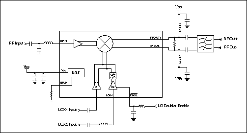
Figure 1. Simplified MAX2683 application circuit block diagram 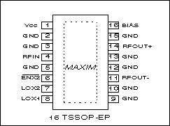
Figure 2. MAX2683 external pins
The MAX2683 requires a DC bias. Although traditional passive mixers use AC signals to turn on the device, active Gilbert cell mixers require a DC power supply. The DC bias is applied to the device in the form of VCC voltage. Enough voltage must be applied to turn on the transistors in the Gilbert cell, otherwise the expected switching action will not occur. The minimum voltage required for the mixer to work is 2.7V. When VCC rises, a simple biasing scheme makes it more difficult to turn on the transistor. As the gain of the mixer increases, the compression point increases accordingly. Because changes in offset will affect linearity, and such changes will affect the level of harmonics and spurious signals generated by the mixer. The change in bias also affects the ft of the transistors in the chip and thus changes the operating frequency range of the mixer. The linearity and supply current of the MAX2683 can be adjusted externally with a resistor connected between BIAS and GND. A resistor rated at 1.2kΩ sets the power supply current to 55mA. Reducing the resistance value can improve the linearity but at the expense of the power supply current. Increasing the resistance value can reduce the power supply current but deteriorate the linearity. We use resistors between 820Ω and 2.0kΩ.
GainThe MAX2683 has a frequency conversion gain. In traditional applications, the output signal will have a higher power than the input signal. Most of the gain of the MAX2683 comes from the emitter-coupled amplifier in the Gilbert unit. The amount of gain achieved varies with frequency, operating temperature, oscillator signal, and bias level. In order to optimize gain and linearity, proper design of the circuit board is the key to all RF and microwave circuits. Keep RF signal lines as short as possible to reduce losses, radiation, and inductance. Use separate, low-inductance vias for each ground pin to connect to the ground plane. For best performance, solder the exposed pad on the device package to the ground plane of the circuit board. The differential open-collector RFOUT- and RFOUT + ports require an external pull-up inductor connected to VCC and an output matching network to optimize gain performance. S parameter of modulation signal input, LO input and RF output is shown in Table 2. Designers can refer to this table to develop optimal matching circuits to meet system specifications.
Oscillator signalThe MAX2683 requires a low oscillator drive level. In a mixer based on the Gilbert unit, the main function of the LO signal is to switch the conduction channel between the external transistors and internal transistors of the four cross-coupled devices. This requires relatively little power. Generally, lower oscillator drive levels can improve the spurious response of Gilbert cell mixers. Increasing the LO power input to the MAX2683 upconverter will saturate the transistors of the four coupling devices and the emitter-coupled pair (actually "quasi-saturation") and reduce linearity. When the LO drive level is smaller than the rated value, the frequency conversion gain is basically unaffected in the range of 5dB to 10dB. When the LO drive level is further reduced, the conversion gain will swing down. Sinusoidal LO signals generally do not have many (harmonic related) frequency components. The typical LO input power when the MAX2683 matches 50Ω is -5dBm.
Working frequency rangeMAX2683 can work in a very wide frequency range. It can be used as both a down converter and an up converter. The frequency of the modulated signal through the four cross-coupled devices of the Gilbert unit can be as high as 3.8 GHz. If the appropriate output is provided to match the network output frequency range can reach 3.6GHz. The MAX2683 has an internal LO frequency doubler. The external LO can operate at full frequency or half frequency. The benefit of operating at half frequency is to reduce the undesired LO leakage signal through the amplifier to the antenna. An internal LO bandpass filter is integrated after the frequency multiplier to help suppress LO harmonic content and spurious mixing signals. The method of using the LO frequency multiplier is to drive ENX2 at a logic low level and connect a half-frequency external LO to the LOX2 port. Drive ENX2 at a logic high level and connect the full-frequency external LO to the LOX1 port to turn off and bypass the LO frequency doubler and LO filter. The advantage of turning off the LO frequency multiplier is that it can reduce the power supply current by 15mA. The maximum frequency range of LOX1 is 3.9GHz, and the frequency range of LOX2 is up to 1.95GHz.
Noise FigureThe Gilbert cell structure is not a low noise structure. The noise figure of the mixer mainly comes from the shot noise of the four collector cross-coupled transistors, the noise of the two transistors of the emitter coupling pair and the thermal noise of the two feedback resistors used by the emitter coupling pair. When the input LO power is very low, the switching action of the LO can affect the noise figure of the mixer. The typical noise figure of the MAX2683 is 12.5dB.
Matching circuit In order to achieve optimal performance, the three ports must be properly matched. Table 1 provides the complete S parameters of these three ports, with a frequency range from 50MHz to 6GHz. Designers can refer to this table to select the best matching circuit to meet system specifications. This application note contains an application circuit schematic showing a three-port typical matching circuit. The input port is matched to 350MHz, the LO port is matched to 1.6GHz, and the output port is matched to 3.55GHz.
Table 1.1 F input S11 parameters
| FREQ. | 5VDC | 5VDC | 3.3VDC | 3.3VDC | FREQ. | 5VDC | 5VDC | 3.3VDC | 3.3VDC | |
| (MHz) | Amplitude | Degree | Amplitude | Degree | (MHz) | Amplitude | Degree | Amplitude | Degree | |
| 50 | 0.868 | -4.4 | 0.868 | -4.5 | 3050 | 0.566 | -147.1 | 0.557 | -154.6 | |
| 100 | 0.851 | -7.7 | 0.850 | -7.9 | 3100 | 0.563 | -147.5 | 0.555 | -157.1 | |
| 150 | 0.817 | -13.9 | 0.813 | -16.4 | 3150 | 0.562 | -151.9 | 0.556 | -159.2 | |
| 200 | 0.801 | -10.1 | 0.797 | -11.6 | 3200 | 0.544 | -154.3 | 0.559 | -162.4 | |
| 250 | 0.816 | -11.8 | 0.814 | -12.5 | 3250 | 0.568 | -156.6 | 0.564 | -164.7 | |
| 300 | 0.831 | -21.1 | 0.830 | -22.5 | 3300 | 0.574 | -160.0 | 0.572 | -167.1 | |
| 350 | 0.791 | -22.4 | 0.789 | -25.0 | 3350 | 0.583 | -162.0 | 0.582 | -169.4 | |
| 400 | 0.770 | -27.4 | 0.578 | -30.0 | 3400 | 0.593 | -164.0 | 0.592 | -171.2 | |
| 450 | 0.710 | -27.2 | 0.639 | -30.6 | 3450 | 0.604 | -167.3 | 0.603 | -174.2 | |
| 500 | 0.715 | -28.3 | 0.700 | -29.9 | 3500 | 0.617 | -169.1 | 0.616 | -176.4 | |
| 550 | 0.713 | -30.8 | 0.701 | -32.2 | 3550 | 0.631 | -171.4 | 0.636 | -178.7 | |
| 600 | 0.705 | -33.3 | 0.691 | -34.8 | 3600 | 0.644 | -173.8 | 0.644 | 179.0 | |
| 650 | 0.698 | -35.8 | 0.688 | -37.5 | 3650 | 0.657 | -176.2 | 0.656 | 176.3 | |
| 700 | 0.690 | -38.4 | 0.680 | -40.1 | 3700 | 0.669 | -178.8 | 0.665 | 173.5 | |
| 750 | 0.682 | -40.9 | 0.672 | -42.6 | 3750 | 0.678 | 178.6 | 0.672 | 170.8 | |
| 800 | 0.672 | -43.1 | 0.662 | -44.9 | 3800 | 0.685 | 175.8 | 0.677 | 168.1 | |
| 850 | 0.665 | -45.0 | 0.654 | -47.0 | 3850 | 0.688 | 172.2 | 0.677 | 165.2 | |
| 900 | 0.660 | -47.0 | 0.648 | -49.1 | 3900 | 0.689 | 170.1 | 0.674 | 162.0 | |
| 950 | 0.654 | -49.1 | 0.643 | -51.3 | 3950 | 0.684 | 167.0 | 0.666 | 158.9 | |
| 1000 | 0.651 | -50.9 | 0.638 | -52.0 | 4000 | 0.675 | 164.0 | 0.654 | 155.0 | |
| 1050 | 0.635 | -55.1 | 0.623 | -58.0 | 4050 | 0.661 | 163.3 | 0.639 | 136.0 | |
| 1100 | 0.635 | -58.1 | 0.622 | -61.5 | 4100 | 0.648 | 160.1 | 0.624 | 153.7 | |
| 1150 | 0.633 | -60.3 | 0.618 | -63.6 | 4150 | 0.632 | 158.2 | 0.608 | 151.2 | |
| 1200 | 0.631 | -61.9 | 0.617 | -65.6 | 4200 | 0.615 | 155.7 | 0.591 | 148.8 | |
| 1250 | 0.631 | -63.5 | 0.619 | -67.1 | 4250 | 0.599 | 152.2 | 0.575 | 146.5 | |
| 1300 | 0.633 | -65.2 | 0.618 | -68.6 | 4300 | 0.584 | 151.9 | 0.561 | 144.4 | |
| 1350 | 0.633 | -66.7 | 0.615 | -70.4 | 4350 | 0.571 | 149.7 | 0.550 | 142.4 | |
| 1400 | 0.630 | -68.7 | 0.615 | -72.4 | 4400 | 0.561 | 147.8 | 0.541 | 140.7 | |
| 1450 | 0.630 | -70.7 | 0.615 | -74.5 | 4450 | 0.553 | 146.7 | 0.535 | 139.0 | |
| 1500 | 0.630 | -72.7 | 0.614 | -76.5 | 4500 | 0.549 | 144.2 | 0.532 | 137.1 | |
| 1550 | 0.629 | -74.8 | 0.614 | -78.1 | 4550 | 0.547 | 140.5 | 0.532 | 133.4 | |
| 1600 | 0.627 | -77.3 | 0.612 | -81.0 | 4600 | 0.548 | 138.8 | 0.534 | 131.8 | |
| 1650 | 0.622 | -79.9 | 0.607 | -82.2 | 4650 | 0.552 | 137.3 | 0.541 | 130.4 | |
| 1700 | 0.619 | -82.5 | 0.604 | -85.9 | 4700 | 0.558 | 135.9 | 0.548 | 129.1 | |
| 1750 | 0.618 | -85.0 | 0.604 | -89.4 | 4750 | 0.566 | 134.4 | 0.556 | 127.5 | |
| 1800 | 0.618 | -87.6 | 0.605 | -92.1 | 4800 | 0.577 | 133.1 | 0.569 | 126.2 | |
| 1850 | 0.616 | -90.5 | 0.604 | -95.0 | 4850 | 0.589 | 131.7 | 0.581 | 124.9 | |
| 1900 | 0.615 | -93.3 | 0.602 | -98.2 | 4900 | 0.604 | 130.4 | 0.595 | 123.6 | |
| 1950 | 0.612 | -96.0 | 0.600 | -101.0 | 4950 | 0.616 | 128.9 | 0.607 | 122.1 | |
| 2000 | 0.612 | -98.7 | 0.601 | -103.2 | 5000 | 0.628 | 127.3 | 0.619 | 120.4 | |
| 2050 | 0.609 | -96.7 | 0.600 | -100.9 | 5050 | 0.671 | 127.8 | 0.644 | 120.9 | |
| 2100 | 0.614 | -98.1 | 0.605 | -102.6 | 5100 | 0.660 | 127.9 | 0.644 | 121.2 | |
| 2150 | 0.620 | -100.0 | 0.613 | -105.1 | 5150 | 0.663 | 127.7 | 0.647 | 121.1 | |
| 2200 | 0.626 | -102.0 | 0.618 | -107.5 | 5200 | 0.668 | 127.2 | 0.651 | 120.1 | |
| 2250 | 0.634 | -105.1 | 0.626 | -109.9 | 5250 | 0.671 | 126.2 | 0.654 | 119.4 | |
| 2300 | 0.640 | -107.5 | 0.632 | -112.4 | 5300 | 0.674 | 124.3 | 0.653 | 117.9 | |
| 2350 | 0.644 | -110.1 | 0.636 | -115.1 | 5350 | 0.672 | 123.1 | 0.650 | 116.1 | |
| 2400 | 0.647 | -112.2 | 0.636 | -118.1 | 5400 | 0.668 | 121.4 | 0.644 | 114.3 | |
| 2450 | 0.642 | -115.0 | 0.634 | -121.0 | 5450 | 0.659 | 119.4 | 0.632 | 112.4 | |
| 2500 | 0.645 | -116.7 | 0.632 | -123.9 | 5500 | 0.647 | 117.7 | 0.618 | 110.9 | |
| 2550 | 0.642 | -119.3 | 0.626 | -126.7 | 5550 | 0.633 | 116.4 | 0.603 | 108.0 | |
| 2600 | 0.636 | -122.0 | 0.616 | -129.5 | 5600 | 0.620 | 114.6 | 0.591 | 107.4 | |
| 2650 | 0.627 | -124.4 | 0.604 | -132.1 | 5650 | 0.608 | 113.1 | 0.581 | 106.5 | |
| 2700 | 0.616 | -127.1 | 0.596 | -134.3 | 5700 | 0.598 | 111.4 | 0.572 | 105.2 | |
| 2750 | 0.608 | -129.2 | 0.590 | -136.4 | 5750 | 0.587 | 109.6 | 0.563 | 103.3 | |
| 2800 | 0.600 | -131.1 | 0.584 | -138.8 | 5800 | 0.577 | 108.1 | 0.554 | 101.4 | |
| 2850 | 0.592 | -134.2 | 0.577 | -141.4 | 5850 | 0.569 | 106.2 | 0.547 | 99.9 | |
| 2900 | 0.583 | -136.7 | 0.569 | -144.1 | 5900 | 0.562 | 105.1 | 0.541 | 98.5 | |
| 2950 | 0.576 | -139.2 | 0.562 | -146.7 | 5950 | 0.556 | 103.0 | 0.557 | 97.1 | |
| 3000 | 0.570 | -141.7 | 0.558 | -149.2 | 6000 | 0.551 | 102.1 | 0.553 | 96.0 |
Table 1.2 LOX1 input S11 parameters
| FREQ. | 5VDC | 5VDC | 3.3VDC | 3.3VDC | FREQ. | 5VDC | 5VDC | 3.3VDC | 3.3VDC | |
| (MHz) | Amplitude | Degree | Amplitude | Degree | (MHz) | Amplitude | Degree | Amplitude | Degree | |
| 50 | 0.648 | -30.3 | 0.648 | -30.4 | 3050 | 0.155 | 173.0 | 0.162 | 170.5 | |
| 100 | 0.460 | -33.8 | 0.459 | -39.9 | 3100 | 0.157 | 169.0 | 0.164 | 165.7 | |
| 150 | 0.382 | -32.2 | 0.381 | -32.2 | 3150 | 0.159 | 165.0 | 0.167 | 161.5 | |
| 200 | 0.343 | -30.7 | 0.342 | -30.7 | 3200 | 0.162 | 161.0 | 0.169 | 157.7 | |
| 250 | 0.318 | -29.8 | 0.318 | -29.0 | 3250 | 0.165 | 158.0 | 0.173 | 154.4 | |
| 300 | 0.301 | -29.6 | 0.300 | -29.8 | 3300 | 0.168 | 155.0 | 0.175 | 151.6 | |
| 350 | 0.287 | -30.0 | 0.287 | -30.2 | 3350 | 0.171 | 152.0 | 0.177 | 149.5 | |
| 400 | 0.276 | -30.7 | 0.276 | -30.9 | 3400 | 0.173 | 150.0 | 0.179 | 147.7 | |
| 450 | 0.266 | -30.7 | 0.267 | -32.1 | 3450 | 0.173 | 149.0 | 0.178 | 146.1 | |
| 500 | 0.260 | -33.3 | 0.261 | 33.6 | 3500 | 0.172 | 147.0 | 0.177 | 144.8 | |
| 550 | 0.260 | -33.3 | 0.261 | -33.6 | 3550 | 0.170 | 146.0 | 0.174 | 143.6 | |
| 600 | 0.255 | -35.1 | 0.250 | -37.0 | 3600 | 0.167 | 145.0 | 0.171 | 142.9 | |
| 650 | 0.250 | -37.0 | 0.248 | -39.4 | 3650 | 0.162 | 145.0 | 0.166 | 142.4 | |
| 700 | 0.245 | -41.1 | 0.245 | -41.5 | 3700 | 0.155 | 145.0 | 0.160 | 142.1 | |
| 750 | 0.244 | -43.4 | 0.245 | -43.8 | 3750 | 0.148 | 144.0 | 0.152 | 141.9 | |
| 800 | 0.244 | -45.6 | 0.245 | -46.1 | 3800 | 0.140 | 144.0 | 0.143 | 141.2 | |
| 850 | 0.250 | -47.7 | 0.246 | -48.3 | 3850 | 0.131 | 144.0 | 0.134 | 141.4 | |
| 900 | 0.245 | -50.0 | 0.247 | -50.7 | 3900 | 0.122 | 144.0 | 0.126 | 140.5 | |
| 950 | 0.246 | -52.3 | 0.247 | -53.3 | 3950 | 0.112 | 143.0 | 0.116 | 139.4 | |
| 1000 | 0.246 | -54.7 | 0.246 | -55.0 | 4000 | 0.102 | 142.0 | 0.106 | 137.9 | |
| 1050 | 0.242 | -59.1 | 0.242 | -60.5 | 4050 | 0.100 | 142.0 | 0.104 | 138.4 | |
| 1100 | 0.240 | -61.5 | 0.240 | -62.3 | 4100 | 0.091 | 141.0 | 0.095 | 137.1 | |
| 1150 | 0.238 | -63.1 | 0.238 | -63.9 | 4150 | 0.083 | 139.0 | 0.087 | 135.1 | |
| 1200 | 0.235 | -64.7 | 0.236 | -65.5 | 4200 | 0.074 | 138.0 | 0.079 | 132.5 | |
| 1250 | 0.233 | -66.2 | 0.233 | -67.1 | 4250 | 0.067 | 135.0 | 0.071 | 129.8 | |
| 1300 | 0.230 | -68.0 | 0.230 | -68.9 | 4300 | 0.060 | 133.0 | 0.065 | 126.7 | |
| 1350 | 0.226 | -69.7 | 0.226 | -70.5 | 4350 | 0.055 | 129.0 | 0.060 | 123.0 | |
| 1400 | 0.222 | -71.5 | 0.222 | -72.5 | 4400 | 0.050 | 126.0 | 0.055 | 119.1 | |
| 1450 | 0.218 | -73.6 | 0.218 | -74.6 | 4450 | 0.046 | 123.0 | 0.051 | 116.3 | |
| 1500 | 0.214 | -75.9 | 0.214 | -77.0 | 4500 | 0.045 | 123.0 | 0.050 | 115.8 | |
| 1550 | 0.209 | -78.4 | 0.211 | -79.5 | 4550 | 0.045 | 124.0 | 0.050 | 117.2 | |
| 1600 | 0.205 | -81.1 | 0.207 | -82.2 | 4600 | 0.047 | 126.0 | 0.053 | 118.8 | |
| 1650 | 0.202 | -84.0 | 0.204 | -85.2 | 4650 | 0.053 | 128.0 | 0.058 | 121.2 | |
| 1700 | 0.199 | -87.1 | 0.200 | -88.4 | 4700 | 0.060 | 129.0 | 0.064 | 122.7 | |
| 1750 | 0.197 | -90.5 | 0.199 | -91.9 | 4750 | 0.068 | 130.0 | 0.072 | 123.9 | |
| 1800 | 0.195 | -94.0 | 0.197 | -95.4 | 4800 | 0.076 | 130.0 | 0.064 | 122.5 | |
| 1850 | 0.195 | -97.4 | 0.197 | -99.0 | 4850 | 0.083 | 130.0 | 0.086 | 125.3 | |
| 1900 | 0.195 | -97.5 | 0.197 | -102.4 | 4900 | 0.091 | 131.0 | 0.094 | 126.4 | |
| 1950 | 0.194 | -101.0 | 0.195 | -106.6 | 4950 | 0.099 | 132.0 | 0.102 | 127.6 | |
| 2000 | 0.193 | -105.0 | 0.195 | -109.5 | 5000 | 0.100 | 133.0 | 0.111 | 128.6 | |
| 2050 | 0.196 | -110.0 | 0.199 | -111.4 | 5050 | 0.122 | 132.0 | 0.125 | 128.0 | |
| 2100 | 0.199 | -112.0 | 0.202 | -113.7 | 5100 | 0.129 | 132.0 | 0.131 | 128.0 | |
| 2150 | 0.201 | -114.0 | 0.204 | -116.0 | 5150 | 0.134 | 133.0 | 0.137 | 129.4 | |
| 2200 | 0.202 | -116.0 | 0.206 | -128.1 | 5200 | 0.139 | 133.0 | 0.142 | 129.2 | |
| 2250 | 0.204 | -118.0 | 0.208 | -120.0 | 5250 | 0.142 | 133.0 | 0.144 | 128.5 | |
| 2300 | 0.205 | -120.0 | 0.209 | -122.0 | 5300 | 0.144 | 132.0 | 0.146 | 127.4 | |
| 2350 | 0.205 | -122.0 | 0.209 | -123.8 | 5350 | 0.144 | 130.0 | 0.146 | 125.5 | |
| 2400 | 0.204 | -123.0 | 0.208 | -125.1 | 5400 | 0.141 | 127.0 | 0.142 | 123.2 | |
| 2450 | 0.202 | -125.0 | 0.206 | -127.4 | 5450 | 0.136 | 125.0 | 0.137 | 120.1 | |
| 2500 | 0.200 | -127.0 | 0.204 | -129.7 | 5500 | 0.129 | 122.0 | 0.131 | 116.5 | |
| 2550 | 0.197 | -129.0 | 0.202 | -132.4 | 5550 | 0.121 | 1118.0 | 0.121 | 112.9 | |
| 2600 | 0.193 | -132.0 | 0.198 | -135.7 | 5600 | 0.110 | 113.0 | 0.117 | 106.4 | |
| 2650 | 0.189 | -136.0 | 0.193 | -139.6 | 5650 | 0.098 | 106.0 | 0.100 | 99.3 | |
| 2700 | 0.183 | -141.0 | 0.187 | -144.4 | 5700 | 0.088 | 99.0 | 0.091 | 190.9 | |
| 2750 | 0.175 | -146.0 | 0.179 | -149.4 | 5750 | 0.079 | 189.0 | 0.083 | 181.1 | |
| 2800 | 0.168 | -151.0 | 0.172 | -154.6 | 5800 | 0.070 | 78.0 | 0.076 | 169.3 | |
| 2850 | 0.162 | -156.0 | 0.167 | -159.9 | 5850 | 0.065 | 63.0 | 0.073 | 155.9 | |
| 2900 | 0.157 | -161.0 | 0.163 | -165.1 | 5900 | 0.063 | 49.0 | 0.073 | 142.0 | |
| 2950 | 0.155 | -167.0 | 0.161 | -170.9 | 5950 | 0.064 | 33.0 | 0.075 | 28.5 | |
| 3000 | 0.153 | -173.0 | 0.160 | -176.7 | 6000 | 0.067 | 18.0 | 0.079 | 16.1 |
Table 1.3 LOX2 input S11 parameters
| FREQ. | 5VDC | 5VDC | 3.3VDC | 3.3VDC | FREQ. | 5VDC | 5VDC | 3.3VDC | 3.3VDC | |
| (MHz) | Amplitude | Degree | Amplitude | Degree | (MHz) | Amplitude | Degree | Amplitude | Degree | |
| 50 | 0.756 | -18.6 | 0.775 | -19.6 | 1550 | 0.304 | -92.1 | 0.306 | -93.3 | |
| 100 | 0.619 | -26.4 | 0.625 | -27.2 | 1600 | 0.301 | -94.5 | 0.304 | -95.7 | |
| 150 | 0.537 | -29.1 | 0.599 | -29.7 | 1650 | 0.299 | -97.1 | 0.303 | -98.4 | |
| 200 | 0.488 | -30.7 | 0.489 | -31.2 | 1700 | 0.299 | -99.8 | 0.302 | -101.1 | |
| 250 | 0.455 | -32.2 | 0.456 | -32.7 | 1750 | 0.298 | -102.3 | 0.300 | -103.9 | |
| 300 | 0.431 | -34.1 | 0.432 | -34.5 | 1800 | 0.298 | -105.4 | 0.301 | -106.7 | |
| 350 | 0.411 | -35.1 | 0.413 | -36.6 | 1850 | 0.299 | -108.1 | 0.301 | -109.5 | |
| 400 | 0.395 | -38.4 | 0.397 | -38.8 | 1900 | 0.299 | -110.8 | 0.303 | -112.2 | |
| 450 | 0.382 | -40.8 | 0.382 | -41.3 | 1950 | 0.302 | -113.4 | 0.305 | -114.7 | |
| 500 | 0.370 | -43.4 | 0.372 | -43.9 | 2000 | 0.303 | -115.9 | 0.307 | -117.4 | |
| 550 | 0.362 | -46.1 | 0.362 | -46.6 | 2050 | 0.310 | -117.1 | 0.314 | -118.6 | |
| 600 | 0.354 | -48.8 | 0.355 | -49.4 | 2100 | 0.315 | -119.2 | 0.319 | -120.7 | |
| 650 | 0.348 | -51.6 | 0.349 | -52.2 | 2150 | 0.305 | -115.0 | 0.324 | -122.7 | |
| 700 | 0.344 | -54.3 | 0.345 | -55.9 | 2200 | 0.324 | -123.0 | 0.329 | -124.6 | |
| 750 | 0.341 | -57.1 | 0.342 | -57.9 | 2250 | 0.327 | -124.8 | 0.332 | -126.4 | |
| 800 | 0.338 | -59.9 | 0.340 | -60.5 | 2300 | 0.330 | -126.5 | 0.335 | -128.2 | |
| 850 | 0.337 | -62.4 | 0.337 | -632.0 | 2350 | 0.334 | -128.1 | 0.327 | -129.9 | |
| 900 | 0.335 | -65.0 | 0.336 | -65.7 | 2400 | 0.335 | -129.7 | 0.339 | -131.4 | |
| 950 | 0.332 | -67.3 | 0.334 | -68.0 | 2450 | 0.335 | -131.4 | 0.337 | -133.2 | |
| 1000 | 0.331 | -69.4 | 0.332 | -70.2 | 2500 | 0.333 | -133.1 | 0.336 | -137.9 | |
| 1050 | 0.326 | -72.1 | 0.327 | -73.4 | 2550 | 0.330 | -134.7 | 0.333 | -136.7 | |
| 1100 | 0.325 | -74.6 | 0.325 | -75.6 | 2600 | 0.325 | -136.8 | 0.330 | -138.7 | |
| 1150 | 0.323 | -76.3 | 0.325 | -77.1 | 2650 | 0.319 | -138.8 | 0.323 | -140.8 | |
| 1200 | 0.322 | -78.1 | 0.323 | -78.9 | 2700 | 0.312 | -140.7 | 0.316 | -142.9 | |
| 1250 | 0.319 | -79.8 | 0.321 | -80.7 | 2750 | 0.305 | -142.6 | 0.309 | -144.9 | |
| 1300 | 0.316 | -81.5 | 0.318 | -82.5 | 2800 | 0.299 | -144.7 | 0.303 | -146.0 | |
| 1350 | 0.327 | -71.1 | 0.315 | -84.4 | 2850 | 0.295 | -146.9 | 0.298 | -147.1 | |
| 1400 | 0.312 | -85.4 | 0.313 | -83.4 | 2900 | 0.291 | -149.1 | 0.293 | -151.4 | |
| 1450 | 0.308 | -87.4 | 0.311 | -88.5 | 2950 | 0.287 | -151.4 | 0.289 | -153.7 | |
| 1500 | 0.306 | -89.7 | 0.309 | -90.9 | 3000 | 0.285 | -153.6 | 0.287 | -156.0 |
Table 1.4 Upconverter output S22 parameters
| FREQ. | 5VDC | 5VDC | 3.3VDC | 3.3VDC | FREQ. | 5VDC | 5VDC | 3.3VDC | 3.3VDC | |
| (MHz) | Amplitude | Degree | Amplitude | Degree | (MHz) | Amplitude | Degree | Amplitude | Degree | |
| 50 | 0.883 | -6.1 | 0.912 | -6.9 | 3050 | 0.739 | 129.7 | 0.738 | 129.6 | |
| 100 | 0.962 | -11.1 | 0.883 | -11.5 | 3100 | 0.729 | 126.8 | 0.729 | 126.8 | |
| 150 | 0.838 | -14.6 | 0.857 | -14.7 | 3150 | 0.710 | 124.5 | 0.711 | 124.7 | |
| 200 | 0.827 | -16.5 | 0.845 | -16.5 | 3200 | 0.686 | 122.6 | 0.687 | 122.8 | |
| 250 | 0.841 | -17.6 | 0.859 | -18.3 | 3250 | 0.654 | 120.8 | 0.657 | 121.1 | |
| 300 | 0.854 | -20.3 | 0.871 | -21.1 | 3300 | 0.620 | 119.0 | 0.625 | 119.4 | |
| 350 | 0.863 | -23.0 | 0.878 | -24.2 | 3350 | 0.589 | 116.8 | 0.595 | 117.4 | |
| 400 | 0.863 | -26.4 | 0.877 | -27.3 | 3400 | 0.564 | 114.6 | 0.570 | 115.0 | |
| 450 | 0.858 | -29.7 | 0.872 | -30.7 | 3450 | 0.543 | 111.7 | 0.551 | 112.2 | |
| 500 | 0.851 | -33.3 | 0.864 | -34.3 | 3500 | 0.532 | 108.6 | 0.541 | 109.1 | |
| 550 | 0.841 | -37.6 | 0.853 | -38.7 | 3550 | 0.530 | 105.6 | 0.541 | 106.2 | |
| 600 | 0.827 | -42.4 | 0.840 | -43.6 | 3600 | 0.539 | 103.6 | 0.550 | 103.8 | |
| 650 | 0.812 | -47.8 | 0.825 | -49.1 | 3650 | 0.558 | 101.0 | 0.570 | 101.8 | |
| 700 | 0.793 | -53.7 | 0.807 | -55.2 | 3700 | 0.583 | 99.9 | 0.597 | 100.5 | |
| 750 | 0.774 | -59.7 | 0.787 | -61.6 | 3750 | 0.613 | 99.4 | 0.628 | 99.9 | |
| 800 | 0.756 | -65.6 | 0.762 | -67.7 | 3800 | 0.644 | 99.4 | 0.660 | 99.8 | |
| 850 | 0.739 | -71.0 | 0.737 | -73.1 | 3850 | 0.672 | 99.7 | 0.690 | 99.9 | |
| 900 | 0.723 | -75.7 | 0.714 | -77.1 | 3900 | 0.694 | 100.4 | 0.713 | 100.2 | |
| 950 | 0.709 | -79.1 | 0.700 | -79.9 | 3950 | 0.707 | 100.1 | 0.726 | 100.3 | |
| 1000 | 0.712 | -83.3 | 0.715 | -83.7 | 4000 | 0.706 | 100.5 | 0.725 | 100.3 | |
| 1050 | 0.715 | -87.0 | 0.711 | -87.6 | 4050 | 0.690 | 103.2 | 0.709 | 102.8 | |
| 1100 | 0.718 | -89.3 | 0.717 | -89.4 | 4100 | 0.667 | 102.9 | 0.686 | 102.3 | |
| 1150 | 0.723 | -91.1 | 0.723 | -91.0 | 4150 | 0.635 | 101.9 | 0.623 | 101.2 | |
| 1200 | 0.725 | -93.0 | 0.727 | -93.2 | 4200 | 0.599 | 100.1 | 0.615 | 99.3 | |
| 1250 | 0.723 | -95.4 | 0.726 | -95.6 | 4250 | 0.563 | 97.3 | 0.578 | 96.2 | |
| 1300 | 0.715 | -98.1 | 0.720 | -98.3 | 4300 | 0.531 | 93.2 | 0.547 | 92.0 | |
| 1350 | 0.702 | -101.0 | 0.708 | -101.0 | 4350 | 0.512 | 87.8 | 0.527 | 86.7 | |
| 1400 | 0.684 | -104.6 | 0.691 | -104.0 | 4400 | 0.505 | 81.7 | 0.521 | 80.6 | |
| 1450 | 0.661 | -108.6 | 0.669 | -109.0 | 4450 | 0.511 | 75.7 | 0.527 | 74.7 | |
| 1500 | 0.633 | -112.8 | 0.642 | -113.0 | 4500 | 0.532 | 70.8 | 0.547 | 69.8 | |
| 1550 | 0.692 | -116.9 | 0.621 | -117.3 | 4550 | 0.562 | 57.3 | 0.576 | 86.4 | |
| 1600 | 0.594 | -121.7 | 0.609 | -122.2 | 4600 | 0.594 | 65.3 | 0.609 | 64.4 | |
| 1650 | 0.577 | -126.5 | 0.589 | -127.0 | 4650 | 0.627 | 64.4 | 0.641 | 63.6 | |
| 1700 | 0.569 | -130.9 | 0.581 | -131.6 | 4700 | 0.656 | 64.7 | 0.669 | 63.9 | |
| 1750 | 0.567 | -135.5 | 0.581 | -136.1 | 4750 | 0.677 | 66.0 | 0.689 | 65.2 | |
| 1800 | 0.571 | -140.1 | 0.585 | -140.7 | 4800 | 0.694 | 67.7 | 0.705 | 67.0 | |
| 1850 | 0.580 | -144.0 | 0.595 | -144.9 | 4850 | 0.703 | 69.8 | 0.711 | 69.0 | |
| 1900 | 0.592 | -148.2 | 0.607 | -148.9 | 4900 | 0.706 | 71.9 | 0.715 | 71.1 | |
| 1950 | 0.608 | -151.0 | 0.623 | -152.6 | 4950 | 0.702 | 73.6 | 0.710 | 72.8 | |
| 2000 | 0.624 | -155.0 | 0.639 | -156.9 | 5000 | 0.691 | 75.0 | 0.699 | 74.2 | |
| 2050 | 0.651 | -156.0 | 0.667 | -157.7 | 5050 | 0.697 | 77.1 | 0.705 | 76.3 | |
| 2100 | 0.674 | -166.5 | 0.689 | -151.3 | 5100 | 0.694 | 76.8 | 0.702 | 75.7 | |
| 2150 | 0.689 | -163.5 | 0.704 | -167.7 | 5150 | 0.684 | 74.5 | 0.692 | 73.6 | |
| 2200 | 0.704 | -166.7 | 0.717 | -167.8 | 5200 | 0.665 | 70.8 | 0.673 | 69.7 | |
| 2250 | 0.711 | -170.3 | 0.723 | -171.5 | 5250 | 0.644 | 65.9 | 0.651 | 64.7 | |
| 2300 | 0.703 | -174.0 | 0.714 | -175.2 | 5300 | 0.624 | 60.2 | 0.631 | 59.0 | |
| 2350 | 0.687 | -177.0 | 0.695 | -178.4 | 5350 | 0.607 | 54.3 | 0.613 | 53.9 | |
| 2400 | 0.669 | -179.9 | 0.677 | 178.6 | 5400 | 0.592 | 48.9 | 0.598 | 47.5 | |
| 2450 | 0.647 | 176.0 | 0.652 | 175.3 | 5450 | 0.581 | 44.5 | 0.585 | 43.3 | |
| 2500 | 0.622 | 173.6 | 0.627 | 172.3 | 5500 | 0.573 | 41.7 | 0.578 | 40.5 | |
| 2550 | 0.604 | 170.5 | 0.609 | 169.2 | 5550 | 0.569 | 40.3 | 0.574 | 39.1 | |
| 2600 | 0.592 | 166.9 | 0.597 | 165.6 | 5600 | 0.567 | 39.7 | 0.570 | 38.6 | |
| 2650 | 0.589 | 163.0 | 0.593 | 161.7 | 5650 | 0.565 | 40.1 | 0.569 | 39.1 | |
| 2700 | 0.594 | 158.8 | 0.590 | 157.7 | 5700 | 0.565 | 41.2 | 0.568 | 40.2 | |
| 2750 | 0.609 | 154.4 | 0.612 | 153.4 | 5750 | 0.566 | 42.6 | 0.569 | 41.7 | |
| 2800 | 0.631 | 149.9 | 0.634 | 149.0 | 5800 | 0.570 | 43.7 | 0.572 | 42.9 | |
| 2850 | 0.656 | 145.3 | 0.658 | 144.6 | 5850 | 0.576 | 45.1 | 0.580 | 44.3 | |
| 2900 | 0.682 | 141.4 | 0.683 | 140.8 | 5900 | 0.583 | 46.0 | 0.586 | 45.5 | |
| 2950 | 0.709 | 137.6 | 0.710 | 137.2 | 5950 | 0.597 | 47.0 | 0.595 | 46.3 | |
| 3000 | 0.729 | 133.9 | 0.728 | 133.6 | 6000 | 0.605 | 47.4 | 0.609 | 46.7 |
The mixer realized by the Gilbert cell structure does not have a high dynamic range. The following two equations describe the linearity dynamic range and the spurious-free dynamic range:
Linear dynamic range = P1dB-[NF + G + 3dB -114 dBm + 10 log10 (BW)]
Spurious-free dynamic range = 2/3 [IP3-G-NF -10 log10 (BW) + 114 dBm]
Where P1dB is the output power of the mixer at 1dB gain compression point (in dBm), NF is the noise figure of the mixer (in dB), and G is the conversion gain of the mixer (in dB) , BW is the bandwidth of the mixer (in dB), and IP3 is the output third-order intercept point (in dB). These equations indicate that the dynamic range is a function of noise figure, output compression point, intercept point, and gain. Because the MAX2683 has a medium conversion gain, its dynamic range is not very low. The linearity of the MAX2683 can be controlled externally through a resistor. Increasing or decreasing the value of the bias resistor will change the linearity of the MAX2683. When changing the bias resistance, a trade-off between linearity and supply current should be made.
Figure 3 shows a typical upconverter application circuit. As indicated in the figure, the mixer is a Gilbert cell-based multiplier with an RF input amplifier. This type of double-balanced mixer provides good port-to-port isolation and no LO signal at the output. The RF output port is configured for differential operation. The RF input and LO input can be driven in single-ended mode. The LO and RF input resistance is 50Ω. The output of the mixer requires an external matching network to convert the high output impedance to a lower impedance to meet the system requirements. This impedance conversion and differential to single-ended structure conversion requires the use of a balanced unbalanced converter or an impedance matching converter. The test data of the application circuit is shown in Table 2. 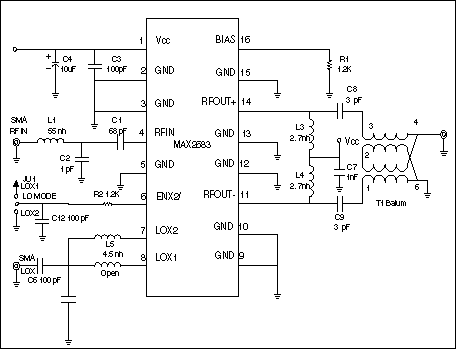
Figure 3. MAX2683 application circuit schematic
(Test conditions: VCC = + 5.0V, RBIAS = 1.2kΩ, / ENX2 \ = GND, fRFIN = 350MHz, PRFIN = -20dBm, fLO = 1600MHz, PLO = -5dBm; the termination resistance of all input and output ports is 50Ω; RFOUT + and RFOUT- are matched to a single-ended 50Ω load; unless otherwise stated, TA = + 25 ° C.)
| PARAMETER | CONDITIONS | TESTED | UNITS | |
| Input Frequency Range | Note 1 | 350 | MHz | |
| RF Output Frequency Range | Note 1 | 3.55 | GHz | |
| LOX2 Frequency Range | 1.6 | GHz | ||
| LOX1 Frequency Range | N / A | GHz | ||
| Conversion Gain | fLOX2 = 1600MHz, fRFOUT = 3.55GHz, VCC = + 5V | 8.6 | dB | |
| Gain VariaTIon over Temperature | TA = -40 ° C to + 85 ° C, VCC = + 5V | TBD | dB | |
| Input 1dB Compression Point | fLOX2 = 1600MHz, fRFOUT = 3.55GHz, VCC = + 5V | -6 | dBm | |
| Input Third-Order Intercept Point | fLOX2 = 1600MHz, fRFOUT = 3.55GHz, VCC = + 5V, Note 2 | +1.3 | dBm | |
| Input Second-Order Intercept Point | fLOX2 = 1600MHz, fRFOUT = 3.55GHz, VCC = + 5V | +42.6 | dBm | |
| Noise Figure | TBD | dB | ||
| RFIN Input Return Loss | At 350 MHz | <-20 | dB | |
| LOX2 Leakage at RFIN | / ENX2 \ = GND | fRFIN = 1 x fLO | -42 | dBm |
| fRFIN = 2 x fLO | -38 | |||
| fRFIN = 3 x fLO | -49 | |||
| LOX1 Leakage at RFIN | / ENX2 \ = Vcc | fRFOUT = 1 x fLO | N / A | dBm |
| LOX2 Leakage at IFOUT +, RFOUT- | / ENX2 \ = GND | fRFOUT = 1 x fLO | -32.7 | dBm |
| fRFOUT = 2 x fLO | -16.4 | |||
| fRFOUT = 3 x fLO | -53.1 | |||
| LOX1 Leakage at IFOUT +, RFOUT- | / ENX2 \ = Vcc | fRFOUT = 1 x fLO | -39 | dBm |
| LOX1, LOX2 Input Return Loss | -18 | dB | ||
annotation
Note 1. This device is specifically designed for this specific frequency range. It may work outside this frequency range but performance cannot be guaranteed.
Note 2. IIP3 was tested with two tone signals of 350MHz and 351MHz, each tone signal -20dBm, fRFLO = 1.6GHz.
Note 3. IIP2 is measured under the conditions of fRFIIN = 350MHz, PRFIN = -20dBm, fLO = 1.6GHz.
Note 4. Optimize input matching so that fRFIIN = 350MHz has the best return loss.
14gram tealight candles can burning 4-4.5hours .and it is made of paraffin wax .100% paraffin wax .
and burning is very goods ,no smoke and no smell
packing have 100pcs/bag and 50bag/ctn ,polybag or box .with client design or my factory design .
price same quality better
quality same price better .
pls be free to contact with me ,Angel 008615081129555
14 Gram Tealight Candle,Slow Burning Tealight Candle,Tealight Candles For Church,Custom Packaging Tealight Candle
Shijiazhuang Zhongya Candle Co,. Ltd. , https://www.zycandlefactory.com