No matter which software you choose for PCB design, there is a general workflow that helps save time and effort. I’ll walk you through the process based on the production flow. Since the interface of Protel is similar to Windows and offers powerful simulation features, it’s widely used among engineers, so I’ll use it as an example in this guide.
Schematic design is the first step in the PCB development process. Many beginners skip this step and jump straight into layout, thinking it saves time. However, this approach often leads to problems later on. For simple boards, experienced designers might get away with it, but for beginners, following the proper sequence is essential. It not only builds good habits but also prevents confusion when dealing with complex circuits.
When creating a schematic, especially using hierarchical design, it's crucial to ensure all files are properly connected. This is important for future modifications and troubleshooting. Different software may have different ways of handling electrical connections, and sometimes a connection appears correct on screen but isn't actually functional. Always use the built-in tools to verify your design before moving forward—this can prevent costly mistakes down the line.
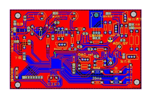
Once the schematic is complete and verified, we move on to the physical board design. The next steps involve setting up the board outline, placing components, routing traces, and making final adjustments. Let’s dive into the key aspects of the board-making process.
1. Define the Board Outline
Creating a closed physical border is essential for component placement and automatic routing. If not done correctly, components may be placed outside the intended area, causing layout issues. Be precise when drawing the outline, as errors here can lead to installation or manufacturing problems. Also, consider using rounded corners instead of sharp ones. Rounded corners reduce stress on the board and make it safer for workers during handling.
2. Component and Network Setup
Placing components and defining their network connections should be straightforward, but mistakes often occur. Pay close attention to warnings and error messages. Common issues include missing component packages, incorrect net assignments, and unused pins. These problems should be fixed early to avoid delays later in the design process.
3. Component Placement
The way components are arranged has a major impact on the performance, stability, and electromagnetic compatibility (EMC) of the final product. Here are some key placement guidelines:
(1) Order of Placement
Start by placing components that are fixed in position, such as connectors, switches, and power jacks. Lock them in place to prevent accidental movement. Next, place large or high-power components like transformers, ICs, and heat-generating parts. Finally, add smaller components like resistors and capacitors.
(2) Heat Dissipation
Proper heat management is critical. High-power components should be spread out rather than clustered together. This helps with cooling and extends the lifespan of the board. Avoid placing electrolytic capacitors near heat sources, as they can degrade faster under high temperatures.
4. Routing
Routing is one of the most technical parts of PCB design. While everyone has their own style, certain rules apply universally:
â—† High-frequency signals should be short and wide to minimize interference.
◆ High-voltage and low-voltage lines must be kept apart. The minimum distance between them depends on the voltage rating—typically 2mm for 2kV, increasing proportionally for higher voltages.
â—† When routing on both sides of the board, keep traces perpendicular or at an angle to avoid crosstalk. Input and output lines should be isolated, ideally with a ground wire in between.
â—† Avoid sharp 90-degree angles in traces. Instead, use larger bends to reduce signal reflection and improve reliability.
â—† Ensure equal length for critical signals like address or data lines to avoid timing issues.
â—† Keep traces on the solder side, especially for through-hole boards, to improve soldering quality.
â—† Minimize the use of vias and jumpers to simplify the board and reduce potential failure points.
â—† Use large pads and thick traces for single-layer boards, and consider adding teardrops for better structural integrity.
â—† Large copper areas should be meshed to prevent voids during wave soldering and reduce thermal stress.
â—† Avoid placing components too close to the edges, as this can cause mechanical stress and breakage.
â—† Always consider ease of manufacturing, testing, and maintenance when placing components.
For analog circuits, grounding is particularly important. Ground noise can severely affect performance, especially in audio amplifiers or high-precision ADC circuits. To reduce this, consider adding a decoupling capacitor at each corner of the board, connecting one end to the ground plane and the other to a mounting hole for shielding.
Electromagnetic compatibility (EMC) is also a growing concern. Components like crystal oscillators can emit unwanted signals, so shielding and filtering are necessary. In high-speed designs, serpentine routing is often used to match trace lengths and eliminate timing mismatches. This technique is common in computer motherboards and high-frequency systems.
5. Final Adjustments
After routing is complete, make final adjustments to text, components, and copper pours. This step should be done after wiring to avoid disrupting the layout. Proper labeling and clear spacing help with production, testing, and future maintenance.
Copper pours are used to fill empty spaces on the board, usually for ground or power planes. They help improve conductivity and reduce noise. However, be careful not to overfill areas where it could cause issues. Always follow the manufacturer’s guidelines for optimal results.
ZTTEK Batteries, For 5G backup base station .Customize the lithium ion battery packs according to the application and product requirements of the customers.
Lithium ion battery integration requires a special set of skill and expertise to optimize the performance and battery life.ZTTEK Batteries , using the most advanced technology delivers the best quality battery packs.
Our batteries are safe to use, better performance, higher shelf life and a very low maintenance cost.
48V200Ah Lithium Ion Battery,Lifepo4 Battery 48V 200Ah,Rechargeable Battery 48V 200Ah,48V 200Ah Lifepo4 Battery Pack
Jiangsu Zhitai New Energy Technology Co.,Ltd , https://www.zttall.com