In today's fast-paced development of electronic technology, most amplifiers are designed using integrated circuits. However, for electronics enthusiasts, it remains a fundamental skill to build a high-fidelity amplifier from discrete components. The power amplifier described in this article is fully built using separate components, featuring a two-stage asymmetric differential circuit in both the input and voltage amplification stages. This design ensures excellent linearity, a wide frequency response, strong resistance to temperature drift and power supply fluctuations, and delivers a warm, natural sound that is truly captivating. It’s definitely worth trying.
First, let’s take a brief look at the circuit principle.
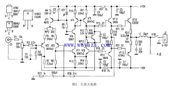
Figure 1 shows the main amplifier circuit. VT2 and VT3 form the input stage differential pair. Meanwhile, VT1, LED1, R4, R9, and C2 create a constant current source for the input stage. When LED1 is properly lit, the voltage difference between the positive and negative terminals remains stable between 1.8V and 2V, which is less noisy than a Zener diode. This is commonly used in power amplifier circuits. The 1.9V voltage difference acts on the emitter junction loop of VT1, resulting in a constant collector-emitter current of approximately 1.9mA (calculated as (1.9V - 0.6V)/680Ω). If the parameters of VT2 and VT3 are perfectly symmetrical, each will carry about 0.95mA of current. Adjusting RP2 changes the feedback resistance of the emitters of VT2 and VT3, leading to symmetrical shifts in their quiescent operating points and ultimately affecting the DC potential at the midpoint of the output stage.
Under normal conditions, the voltage drop across R7 and R8 is around 2.1V (calculated as 2.2kΩ × 0.95mA), which serves as the bias voltage for the emitter junctions of the voltage amplification stage differential pair VT7 and VT8. The current through the VT7 and VT8 pairs is roughly 4.5mA ((2.1V - 0.6V)/R13). VT4 and VT5 form a current mirror load for the differential voltage amplification stages of VT7 and VT8, while VT6 acts as a load resistor for VT7.
VT9, R12, and RP3 make up the bias circuit for the push and output stages. They also provide temperature feedback control for the final power transistors. By adjusting RP3, the voltage between the base and emitter of VT9 can be changed, thereby altering the quiescent bias current of the push and output stages. Moreover, since VT9 is mounted on the same heat sink as the power transistors VT12 and VT13, it helps regulate their temperature. If the output current of VT12 and VT13 increases, the base-emitter current of VT9 rises, causing a drop in the collector-emitter voltage when the temperature exceeds the safe limit. This reduces the static output current of the push and output stages, keeping the power transistors within a safe operating range.
VT10 and VT11 form the push stage, and the DC voltage drop across the emitter resistors R19 and R20 provides the bias voltage for the power output transistors VT12 and VT13. RP3 can be adjusted to fine-tune the static output current of these transistors. R26, C9, and R27 create an AC feedback network for this stage, giving the entire amplifier a voltage gain of 52 times (Av+ = 1 + R26/R27 = 52). The feedback point is selected at the symmetrical midpoint of the push stage, minimizing the impact of the speaker on the small signal input stage. Compared to the traditional method of taking feedback from the output midpoint, this configuration significantly improves sound quality, enhances control, and offers better transient response.
LVDS Automotive High Frequency Cable Assembly
Lvds Automotive High Frequency Cable Assembly,Electronic Components Connectors,Electronic Connectors,Electronics Connectors
Dongguan Zhuoyuexin Automotive Electronics Co.,Ltd , https://www.zyx-fakra.com