The emergence of digital power supply allows engineers to optimize loop compensation. Loop compensation mechanisms can also be used by engineers for application analysis. The loop data converter determines the interference in the power supply output by fine-tuning the duty cycle of the digital pulse width modulator (PWM). The loop control component provides the incentives and responses needed to determine the power frequency characteristics. The digital system can assist in analysis and can memorize the optimal compensation parameters under different line and load conditions. In application, the digital system can set the optimal compensation parameters in the digital power supply solution by identifying the line and load conditions it has memorized, or notify the power supply system when a special operating mode is encountered.
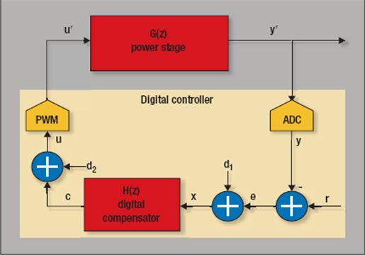
Figure 1. Schematic diagram of two possible excitation signal injection points (d1 and d2) for measuring frequency response.
For power loop analysis, we can inject a signal with a sequence of sine waves of a specific amplitude and frequency. By adding a sine wave sequence to a variable in the control loop, we can inject this sequence into the feedback loop. At another place in the loop, the response of the injected sequence can be measured by performing a Discrete Fourier Transform (DFT) on the frequency of the injected sequence. If the DFT operation includes both sine and cosine elements, the amplitude and phase of the response can be calculated from the orthogonal results of the DFT operation.
Loop analysis using digital power controllers
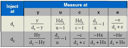
The technique of measuring the frequency response of a feedback control system is basically the same, regardless of whether the system to be measured is a continuous-time analog system or a discrete-time digital system. Figure 1 shows two possible positions for injecting an excited sine wave signal, indicated by d1 and d2, respectively. Figure 1 also shows the possible positions of the measured excitation signal response, indicated by y, u, c, x, and e, respectively.
If the excitation sine wave signal is injected at the d1 position, the sine wave is added to the error calculation result as a digital signal. The error calculation is very simple, ie the difference between the digital voltage output and the preferred voltage output equivalent digital output. In the same way, d2 can be added to the digital value to generate the pulse width of the digital PWM.
A more comprehensive analysis of transmission gains can be found in several complete references listed at the end of this article (1-6). Nevertheless, we have tabulated the different gains for each specific measurement position shown in Figure 1.
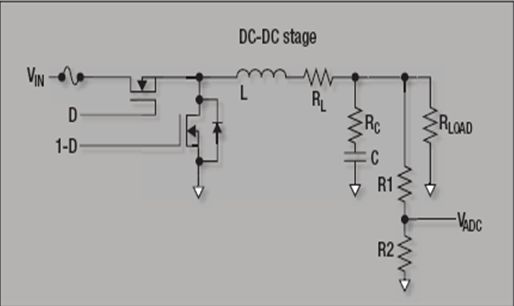
Figure 2. The small-signal AC transfer function of the buck converter is derived from this model.
Digital controller design
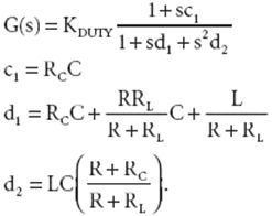
Let's define a buck converter stage as shown in Figure 2. For this converter, the equation for its small-signal AC transfer function is as follows:
Equation 1
To get a typical value, set each parameter to:
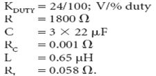
This generates a zero power level at 2.4 MHz and produces a second-order complex pole at 24.3 kHz with a Q value of 1.68. The purpose of defining the gain is to simulate the difference between measurement methods; the input to the power stage is the percentage of the duty cycle, and the output unit is volts (V).
The controller includes a two-pole, two-zero digital compensator. In this example, the compensator's zero is set to 30 kHz and the poles are set to zero (to form an integrator) and 300 kHz. The gain of the compensator is defined as 43dB at 1kHz. The digital sampling rate is set to 700kHz PWM switching frequency.
Equation 2
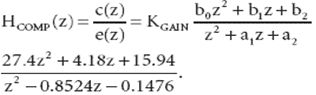
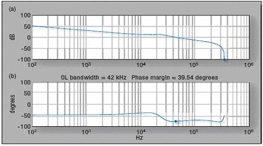
Figure 3 shows an analog open-loop transfer function for a typical system. We can use this system to evaluate the four transmission gains defined in Figure 4. The G/(1+GH) trace has the lowest gain and, in the best case, has a gain of -20 dB. This shows that you should inject a large signal to get a small amplitude at the measurement point. This option is not particularly ideal. The 1 (1+GH) trace has a lower gain at low frequencies, but the gain at high frequencies is equal to or greater than 1.0. Similarly, we can see that the GH(1+GH) trace has good gain at low frequencies, but the gain is lower at high frequencies. Finally, the H/(1+GH) trace is the transmission gain that we can see when injecting the excitation signal at the input of the compensator and measuring it at the output of the compensator. In this case we use the gain in the compensator with the highest measured gain.
The analog open-loop transfer function of the buck converter shown in FIG. 3 and FIG. 2 has an open-loop bandwidth of 42 kHz and a phase margin of 39.54 degrees.
Figure 4. Transmission gain calculation for four measurement options for the buck converter model shown in Figure 2.
Bode Analysis Design Tool
Using the TMS320F2808 and a PC-based design tool, we developed an internal circuit loop analysis system for reference design of digital telecommunication rectifiers. The PC communicates with the power supply via an RS-232 interface. Telecommunication rectifiers have three loops that can be analyzed using an internal circuit loop analysis system, namely power factor correction (PFC) voltage loops, PFC current loops, and DC-DC voltage loops. We have defined related commands to select these three loops in the power system.
Open loop G(f)H(f) for each measurement option is calculated.
To highlight the characteristics of the analysis system, we chose an injection node and a response measurement node. We specified the start frequency, stop frequency, frequency step number, injection amplitude, dwell samples, and measurement sample number in the analysis. The PC test program sends commands to the digital controller, measuring the frequency response of each frequency step. At the end of each measurement, the digital controller returns two cumulative sine and cosine coefficients for that frequency. The PC program calculates the complex open loop transfer function and then plots the amplitude and phase of the frequency.
Since the power stage compensator is in digital form, the test program can query the digital controller to obtain the compensator coefficients and then calculate the exact frequency response of the compensator. Once the frequency response of the compensator is known, the open-loop transfer function will be factorized to calculate the power level transfer function.
After these measurements and calculations were performed, the user chose to display the frequency response of the power stage, the frequency response of the digital compensator, and the frequency response of the open-loop or closed-loop system.
After the loop analysis measurement is performed and the frequency response of the analog power stage is determined, the Bode tool can be used to quickly inspect the results of the compensator coefficient changes; due to the digital nature of the compensator, the result is deterministic.
The benefits of digital power analysis
CNC power loop analysis is useful during power design, manufacturing, and system operation. Similar to current analog power supply designs, power supply designers determine (digital) compensation under expected operating conditions. The difference is that analog power designers use network analyzers in their analysis and adjust the compensation network's resistance and capacitance, while digital power designers can adjust the compensation conditions in the virtual space to get the best results. At the same time, the designer can ensure that the compensator is very accurate without the circuit tolerance of the analog components.
During the manufacturing process, each power supply can optimize the frequency response based on the characteristics of the power stage components without being affected by the expected changes. This makes power stage components more widely applicable without sacrificing the frequency response of the power supply.
One of the major factors that may affect power supply design is system designers. System designers may place many capacitors around different components to assist with bypass performance or to perform local energy storage. In many cases, such abuse of capacitance actually reduces the frequency response of the power supply.
Figure 5 shows an example of adding different capacitors to the output of a 1-kW telecommunication rectifier without adjusting the compensation. After increasing the capacitance, the gain of the system will decrease, and thus the frequency response may not meet the system requirements. In-system frequency analysis helps re-compensate the power supply to accommodate the unexpected capacitance. If this is not done, at least an indication should be made that the power frequency response may not be satisfactory.
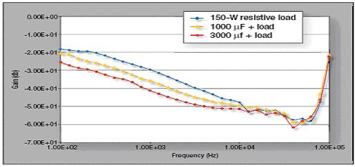
Figure 5. Adding different capacitors to a 1-kW telecom rectifier without compensation adjustment affects the DC-DC closed-loop gain response of the rectifier.
Development prospects
Techniques for measuring power level transfer functions are very efficient in storage and mixed integer programming. If the nodes that inject the excitation signal and measure the response are selected correctly, the technology also has a good SNR characteristic. Finally, this measurement technology allows designers to convert loop compensation measurements and calculations into a factory floor production or end-user application.
Wire Feeding Roller is part of the spraying system.
Wire Feeding Roller
Wire Feeding Roller,Welding Wire Feed Roller,Wire Feeder Roller,Wire Feed Drive Roller
Shaoxing Tianlong Tin Materials Co.,Ltd. , https://www.tianlongspray.com