Tags: DVI TMDS
This article refers to the address: http://
0 Preface
Currently, analog interfaces have become the standard for desktop displays, but the popularity of PFD displays requires a fully digital interface, because for flat-panel displays, the analog interface is completely unnecessary, and the digital interface does not have to adjust the clock and phase, and has There is no loss in signal transmission. With the advancement of digital flat panel displays, the need for digital graphics connections has become clear. The DVI digital video interface standard proposed by the Digital Display Working Group (DDWG) has solved the above problems well, and is also compatible with the traditional VGA interface and DVI interface. It is a promising PC video interface. standard.
1 DVI interface system
DVI mainly uses TMDS (Transition Minimized Differential Signaling) technology to transmit digital signals. TMDS uses advanced coding algorithms to encode 8-bit data (each of the primary color signals in R, G, and B) into 10-bit data by minimum conversion. (Includes line sync information, clock information, data DE, error correction, etc.), and after DC balance, uses differential signals to transmit data. It has better electromagnetic compatibility than LVDS and TTL, and can realize long-distance, high-quality digital signal transmission with low-cost dedicated cable. The connection transmission structure of TMDS technology is shown in Figure 1.
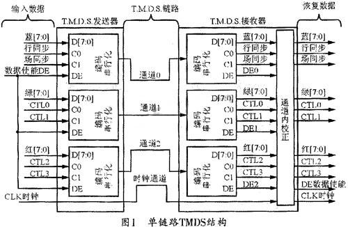
DVI digital signal transmission has two methods: single link (Single Link) and dual link (Dual Link). When using a single connection, only the channels 1, 2, and 3 shown in Figure 1 are transmitted, and the transmission rate is up to 4.9 Gbps, and the dual connection is up to 9.9 Gbps.
2 DVI interface application
The general block diagram of the DVI application system is shown in Figure 2. The DVI interface is the DVI output of the graphics card; the TFP401A is the receiving chip of the TMDS signal, which is the core of the entire receiving system; the AT2402 is the I2C serial bus memory of the ATMEL company, which is used to store the EDID data.
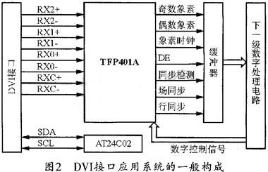
The TMDS link transmitter of the DVI interface is generally directly integrated by the display control chip. Display adapters with DVI function have been integrated into the TDMS transmitter, and the performance generally meets the DVI1.0 specification; the graphics card with ATI's display control chip as the core is generally responsible for TDMS signaling by the on-board Silicon Image Si1164 chip. . The TDMS receiver of the DVI interface and signal decoding are the most important applications. This paper introduces the TDMS receiving system with TFP401A as the core.
2.1 Functional structure of the TFP401A receiver
The TFP401A is a TDMS signal receiving chip from TI's PanelBus flat panel display product line. It features an advanced 0.18μm EPIC-5TM CMOS process, 1.8V core voltage and 3.3VI/O voltage, low noise and low power consumption, and its PowerPADTM package technology guarantees thermal stability of the chip operation. It is mainly used for LCD desktop displays, and can also be applied to other high-speed digital video applications.
The main functions of the TFP401A are as follows:
â—‡ Support SXGA (1280 X 1024, 80 Hz) pixels, the clock can be up to 112 MHz;
â—‡ Support 24-bit (224=16.7 M) true color (1 pixel/clock or 2pixel/clock);
a terminal impedance matching resistor manufactured by a laser precision process in the crucible;
â—‡ 4 times oversampling technology; jitter suppression can reach 1 pixel / clock;
â—‡ has line sync signal jitter suppression.
The specific pin signals of the TFP401A can be found in the data sheet. The internal structure and function are shown in Figure 3. The input RX(2~0)+- and RXC+- are the 4-way TMDS signals from the host that are serial-to-parallel-encoded. And its output signal mainly has odd and even pixel signals (QE[0:23], QO[0:23]), pixel clock ODCK, pixel effective DE, line/field synchronization (HSYN/VSYN) and Synchronous detection of SCDT, etc.
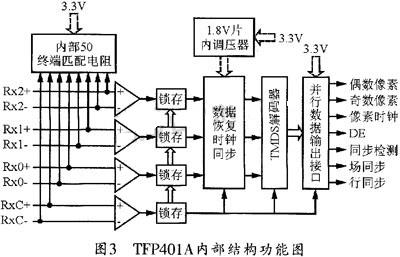
The TFP 401A determines the activation state of the link by detecting the state change of the DE signal. When the 106 pixel clock has passed, if the DE state has not changed, the link is considered to be inactive, and the system outputs SCDT=0. In the case of SCDT=0, if it is found that the DE signal has two transitions within 1024 pixel clocks, the link is considered to be activated, and SCDT=1. The device's synchronous detection indication signal (SCDT) can be directly connected to its output driver power control terminal (PDO), which allows the chip to automatically manage the power supply of the output driver according to the activation of the TMDS link. The PD provided by the TFP401A The terminal can be used to control the power supply of the entire chip. The terminal is a system-level power management control terminal. It is generally not recommended to directly connect to the SCDT terminal of the chip during design.
2.2 TFP401A output control signal connection
The output control signal terminals CTL1, CTL2, CTL3, VSYNC, HSYNC, and DE of the TFP401A should generally be driven by Schmitt triggers to ensure that the low-voltage differential signals can be transmitted to the next-level device. The SN74LV14A can be used to design this function. The data signal of the output address must have sufficient driving capability, which needs to be driven before being passed to the signal processing circuit. The wood design is to increase the driving capability by buffering the driving chip 74F244.
2.3 TFP401A chip power supply and decoupling
The TFP401A-based system is mainly divided into four parts: analog comparator, phase-locked loop (PLL), digital circuit and output signal driver. The VCO (Voltage Controlled Oscillator) inside the PLL loop is most sensitive to the fluctuation of the power supply, and because it needs to provide the reference clock for the circuit, the PLL has the highest power requirement; the second is the analog comparator; the digital circuit has relatively high power requirements. Low, but the most power consumption. In the TFP401A application guide provided by TI, the power supply is uniformly powered, and the four power supplies are isolated by four inductors, but this will increase the size and weight of the circuit, and the presence of the inductor will also cause interference to the analog circuit. Therefore, in the case where strict control of the cost is not required, it is recommended to use the power supply method as shown in FIG. 4, that is, to supply power to the analog and digital circuits by using two TPS7333Qs respectively. The TPS7333Q is a low-dropout linear regulator circuit with high power supply noise rejection and a 3.3 V supply voltage for the chip. AVDD and PVDD are the comparator power supply and PLL power supply of the analog loop respectively; OVDD and DVDD are the output drive power and digital power supply of the digital loop, respectively. By separately supplying power to the analog and digital, and further stringing a small inductor to the circuit with higher power requirements to further smooth the power ripple, the circuit volume can be greatly reduced and the power quality can be improved.
2.4 TFP401A heat dissipation and copper application
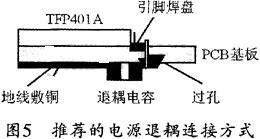
PowerPADTM packaging technology makes the TFP401A highly thermally stable. The bottom of the chip has a thermal pad of approximately 25 mm. It is recommended to connect it to the signal ground of the PCB during soldering. This provides better EMI performance and improved line swell current immunity to power supply noise. Strong. In the specific operation, a through-hole pad with a diameter of about 100 mm can be placed at the position of the heat-dissipation pad of the chip, and the inside of the chip is filled with solder and connected with the ground wire of the bottom layer to pass the heat generated by the chip through the through hole. The filled solder is transferred to the back and radiated.
Since the TFP401A is usually used in a high-frequency digital-analog mixed-signal environment, it is recommended to apply copper to the top and bottom of the PCB. On the one hand, large-scale ground wire copper can provide a relatively quiet working environment for the chip, and on the other hand, it is beneficial to the heat dissipation of the chip. Although the TFP401A provides four types of power pins and ground pins for analog and digital on the chip, it is difficult to separate the four ground wires and ground them at one point. Generally, all the grounding pins are connected to the ground copper, and the currents on the copper wire are grounded by the via holes, so that most of the ground currents of the four types of ground wires flow along different paths, and finally merge to Just one place.
2.5 Signal trace and impedance matching
In the DVI link structure, the link clock can reach 650 MHz at XGA 60Hz field rate, and the internal sampling clock of the chip will reach 615 GHz. At such high operating frequencies, the chip becomes sensitive to the way the circuit is routed and the pad size. It is roughly estimated that there is about 1 nH of inductance on a 1 mm wire in a high-frequency circuit, so that a 10 mm wire will produce 40Ω impedance at a link frequency of 650 MHz, so the signal input of the chip Keep your feet as close as possible to the DVI interface socket. The signal lines of different signal channels should avoid parallel traces, and there should be a ground line between the signal lines for isolation to avoid crosstalk between high frequency signals as much as possible.
At the signal output of the chip, the 86 MHz square wave signal can be output on the clock output pin (ODCK), and the pixel data output pin often operates at an operating frequency higher than 25 MHz. If the lead data of the pixel data to the display control circuit is long, the impedance matching problem of the output signal should be considered. Due to the reflection, overshoot, undershoot of the signal and the influence of the surrounding environment, if the matching is not performed, it is easy to make the control circuit of the display data receiving end logically confusing. Therefore, in practical applications, it is necessary to string a matching resistor in the vicinity of each signal output end of the TFP401A to suppress the secondary reflection of the signal. The resistance can generally be selected between 33 and 100 Ω. The author chose 33Ω matching resistor for the design, and the corresponding signal connection width is 20 mil.
3 VESA standard analysis
At present, the dual display interface graphics card on the market usually uses a 15-pin VGA interface as the main display interface of the system, and the DVI interface as an auxiliary display interface. In the case where the display is not connected to the DVI interface, the display signal of the auxiliary channel is turned off. In order to properly start and use DVI interface signals, it is often necessary to master several important VESA display standards.
3.1 DDC interface design
DDC (DisplayDataChannel) displays the data channel. In the DVI protocol, DDC2B is used. This is a communication standard established on the I2C bus protocol. The host and the display device query and transmit EDID data through the DDC channel to realize the correct use of the display device. Plug and play. At present, the main DDC standards are as follows:
DDC1: The original DDC standard is a one-way data channel that continuously transmits EDID information from the display to the host.
DDC2: A two-way data exchange channel that allows the host to read the display extension display information EDID.
DDC2B: Allows the host and display to exchange code in both directions, and the host can send display control commands to the display.
DDC2B+: A two-way transmission data channel that allows the host to control the display. The standard has a wider communication bandwidth and can even be connected to other peripherals such as joysticks and mice.
The core circuit that implements the DDC interface is the EEPROM circuit of the serial I2C bus. The key to circuit design is to meet the requirements of the I2C bus standard. To ensure circuit safety during design, a current limiting resistor of 50 to 100 Ω must be connected in series.
3.2 EDID standard
Implementing a DDC interface generally requires writing EDID data. E-DID is a data structure with many different variables that define the identity of the display and various display capabilities to the host, and is independent of the data transfer protocol of the display and the host. The key to writing EDID is to clearly understand the EDID data format and extended display identification data, which includes the manufacturer of the display device, the product serial number, the EDID version information, etc., and also indicates the display capabilities supported by the display device, including the display. The resolution, the field frequency, the range of the horizontal frequency, the timing composition of the blanking signal, and the displayed chromaticity coefficient. These parameters are stored in a dedicated 1 Kb EEROM memory in the display (ie, the E-DID data structure is 128 Bytes). The PC host and display access the data in the memory through the DDC data line to determine display attributes (such as resolution, aspect ratio, etc.) of the display.
3.3 HPD (HotPlugDetectionl hot plug detection
The HPD is used to monitor the access or removal of the display device. When the system detects that a display device is connected by HPD, it will access its EDID data through the DDC channel in order to correctly drive the newly connected display device.
The DVI interface protocol requires that the DVI interface compatible display device be capable of providing EDID 1.2 or EDID 2.0 data. The system should start or when the user modifies the monitor display properties, the EDID data should be queried through the DDC channel. If the connected device is faulty or does not detect EDID data, the system will not start the signal output of the DVI interface. In practical applications, the EDID data should be written to the EEPROM of an I2C bus interface. The clock line (SCL), data line (SDA), and pins 6 and 7 of the DVI interface socket can be connected. Connect the 16th pin of the DVI interface socket to the HDD signal of the display device by connecting the 1 kΩ pull-up resistor to the 14th pin (DVI interface DDC+5V power supply terminal).
4 Conclusion
This paper analyzes the architecture and basic principles of DVI from the perspective of engineering application, and introduces an experimentally validated application design method of DVI receiving system. The purpose is to enable readers to quickly grasp the communication protocol of DVI and its application circuit. Designed to extract video information from the interface, free from the study of the complex hardware principles inside the computer, so that the high-quality digital video information of the DVI interface can be developed and utilized according to user requirements.
About Silicone Straw :
Straw is common in our life,when we would like to drink some juice,coffe,beer etc,and if you want to elegant to drink it,in this time we can use it.But when we want to drink some hot drinks what can we do it?Yes,use the silicone straw.The temperature at which silicone straw is -40- +240℃ and it is made of food grade silicone.Silicone texture is soft,it is not like stainless steel or plastic that to hurt our mouth.More inportant,the silicone can be reusable and it is be easy to clean.Now,more and more people use silicone straw in all over the world.
Why don't you choose our silicone straw to expend your business?
Silicone Straw introduction:
1.Product name:Silicone Drinking Straw,Food Grade Silicone Straw, Silicone Straw Tips ,Clear Silicone Straw,Silicone Reusable Straw.
2.Place of origin:Guangdong China
3.Color:any pantone color
4.Logo:Printing,debossed,embossed
5.MOQ:500pcs.
6.Package:1 pcs/opp,customized design is available.
7.Design:Customized/stock
8.Certification:FDA,LFGB,SGS,ROHS,etc.
9.Usage:For drinks/Bar accessories.
10.Silicone Straw photo's for reference.

Silicone Straw
Silicone Drinking Straw,Food Grade Silicone Straw,Silicone Straw Tips,Clear Silicone Straw,Silicone Reusable Straw
OK Silicone Gift Co., Ltd. , https://www.oemsiliconegift.com