This paper mainly explains the principle of the traditional Gardner algorithm, then gives the improved design and FPGA implementation method. Finally, the simulation and analysis of the results prove the correctness and feasibility of the design.
0 Preface
In digital communication, the bit synchronization performance directly affects the quality of the receiver, which is the focus and hot issue of communication technology research. In the communication system, the receiving end generates a timing pulse sequence having the same rate as the transmitting baseband signal and having the same phase as the optimal decision timing. This process is called bit synchronization. Common bit synchronization methods include filtering and phase discrimination. The filtering method transforms the received waveform to contain bit synchronization information, and then filters out through the narrowband filter. The disadvantage is that it is only applicable to narrowband signals. The most commonly used method of bit synchronization is phase-detection, including phase-locking and interpolation. The phase-locked method uses a traditional phase-locked loop, which requires constant adjustment of the frequency and phase of the local clock, and is not suitable for baseband symbol synchronization over a wide rate range. The interpolation method uses the interpolation principle of the digital signal to directly obtain the value and phase of the optimal decision point by calculation.
The Gardner algorithm is based on the principle of interpolation, and adjusts the parameters of the interpolation calculation through the timing loop to track and lock the bit synchronization signal. The advantage of this algorithm is that it does not need to change the local sampling clock, and can adapt to a wide range of speeds. The baseband signal has the advantage that it is irreplaceable by traditional methods. The implementation method of Gardner algorithm provides the basis for the application of the algorithm. The Farrow structure is very suitable for implementing the core of the Gardner algorithm, that is, the interpolation filter part. The advantage is that the resource is less occupied, and the filter coefficients are calculated in real time, which is convenient for interpolation parameter adjustment. Timing error detection, but the timing information is required to have decision information in the signal and is sensitive to carrier phase deviation. Insufficient improvements have been made, and the GA-TED (Gardner TIming Error DetecTIon) algorithm has been proposed, which has the advantage of not requiring predictive decision information, independent of carrier synchronization, and is suitable for FPGA implementation. The improved Gardner algorithm is applied to the M-PSK system. The Gardner algorithm's anti-noise capability is improved, which reduces the local clock requirements.
This paper is based on FPGA platform and adopts Gardner algorithm design. The interpolation filter adopts Farrow structure and the timing error detection adopts GA-TED algorithm. At the same time, the structure of the traditional Gardner algorithm is improved, so that the parameters of the loop filter and NCO can be set by the external controller to adapt to the baseband symbols of different rates, and the design scheme of the universal bit synchronizer is realized. In addition, this design optimizes the FPGA code and saves a lot of hardware resources. Finally, the simulation and analysis are carried out, and the simulation results are given, which proves the feasibility of the scheme.
1 Traditional Gardner algorithm and improvement
1.1 Basic Principles of Traditional Gardner Algorithm
The structure of the traditional Gardner algorithm is shown in Figure 1.
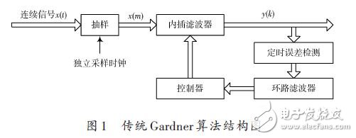
In Fig. 1, the input continuous time signal x(t) symbol period is T, and the frequency band is limited. Under the condition that the Nyquist theorem is satisfied, the receiving end samples x(t) with an independent clock. The interpolation filter calculates the interpolation value y(k), sends it to the timing loop for error feedback and parameter adjustment, and sends it to the sample decider of the demodulator together with the bit synchronization pulse BS output by the controller.
The timing loop includes timing error detection, loop filters, and a controller. The timing error detection extracts the error of the interpolation time and the optimal decision time; the error is filtered by the loop filter to send the high frequency noise to the controller; the controller calculates the interpolation time (that is, the 2 times frequency of the bit synchronization signal) and the error interval. The interpolation time and the error interval are used to adjust the coefficients of the interpolation filter so that the interpolation time is as close as possible to the optimal decision point, and finally the bit synchronization signal is extracted.
1.2 Improved Gardner algorithm structure
As can be seen from the previous section, the traditional Gardner algorithm cannot meet the bit synchronization requirements of baseband signals in a wider rate range. In order to achieve this requirement, the design of the algorithm is improved on the basis of the FPGA platform. The improved structure is shown in Figure 2.
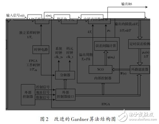
In Figure 2, the interpolation filter is implemented by a Farrow-structured FIR filter, and the filter coefficients are calculated in real time. The timing error detection uses a GA-TED algorithm that is independent of the carrier and has fewer sampling points. The loop filter and internal controller can be The external controller sets the parameters. When the baseband symbol rate changes, the corresponding parameters can change accordingly. Therefore, this design can meet the versatility requirements of the bit synchronizer.
The synchronizer works as follows: The external controller sets the corresponding parameters according to the baseband symbol rate, and sends the control, address and data signals to the frequency divider, loop filter and internal controller through the external controller interface. The clock circuit provides the sampling clock and the FPGA clock respectively. The FPGA working clock generates a clock of the required frequency through the frequency divider on-chip for use by each module of the FPGA. The input continuous time signal x(t) is sampled by an independent clocked ADC, converted to an 8-bit digital signal and sent to the FPGA, symbolized and converted to a signed digital sequence for transmission to the interpolation filter block. The interpolation filter calculates the interpolation value y(kTI) of the optimum decision point at each interpolation time kTI based on the sampled value of the input signal and the parameter μk given by the internal controller. The timing error detection calculates the error μτ (n) and outputs it to the loop filter. The loop filter filters out the noise and sends the error information to the internal controller based on the current parameter settings. The internal controller takes the NCO as the core, adjusts the interpolation time kTi according to the processed error information and the set frequency word parameter, makes it as close as possible to the optimal decision time, and outputs the bit synchronization pulse BS, and simultaneously calculates the error interval μk The interpolation filter is given, the interpolation value is calculated, and the recovery of the timing information is finally completed.
Hengstar offers a range of fully enclosed Industrial Monitors for industrial operator terminals and a variety of factory applications. With a stainless steel or black powder coated enclosure, and IP65 grade connectors, these monitors can be wholly water-proof and dust-proof. Hengstar also offer a variety of industrial keyboard, mounting arms, KVM extender, and fanless Pc Motherboard options to create a full, stand-alone workstation.
Waterproof Monitor,Waterproof Touch Screen,Waterproof Computer Monitor,Waterproof Touch Screen Monitor
Shenzhen Hengstar Technology Co., Ltd. , https://www.angeltondal.com