A current monitoring circuit for lithium batteries is proposed. The current is sampled by introducing a sensitive resistor in the lithium battery power supply loop, and the switch-capacitor operational amplifier and high-speed comparator are used to convert the analog signal to the digital signal. . The precise current amount calculation in the processor can protect the overcurrent and short circuit currents, and can also be used to accurately calculate the relevant parameters such as battery impedance and power. The circuit is based on a 0.18 m CMOS process with a supply voltage of 2.5 V. The circuit has been simulated and verified. The results show that the circuit can realize the sampling and encoding function of current in the range of application temperature range of -40 °C ~ +125 °C, and can judge the charging and discharging action.
As a new clean and renewable secondary energy source, lithium batteries need to accurately monitor their current, voltage and temperature parameters, and make appropriate protection circuits. For handheld devices, it is more necessary to pursue high precision and low power consumption, thereby reducing the "excessive" use of lithium batteries and prolonging the service life.
The circuit designed in this paper introduces a sensitive resistor in the lithium battery power supply loop to monitor the current, provide charging and discharging tips for the system, and can be used for power calculation and protection control.
This paper will elaborate on the principle of the current monitoring system and the internal circuit structure, and give the H-spice simulation results and related conclusions.
1 Current monitoring circuit designed in this paper
The analog to digital converter (ADC) consists of sampling, quantization, and encoding. The block diagram of the lithium battery current monitoring system designed in this paper is shown in Figure 1. Among them, the capacitor and the AMP amplifier form a switching capacitor sampling circuit, the C0MP high-speed comparator quantizes the data, and the processor performs digital logic control and encoding on the circuit. The bias circuit provides an AMP amplifier self-starting branch and generates Vbe1 and Vbe4. The clock module controls system switches, including LII, LI2, LI5, LI6, and LI38. The processor outputs a digital signal Logic Control that changes the quantization capacitance.
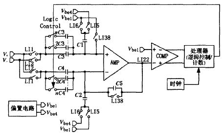
Figure 1 Lithium battery current monitoring system block diagram
1.1 Switched Capacitor Sampling Circuit
As shown in Figure 2, sampling is performed by a sensitive resistor between V+ and V-; Vbe1 and Vbe4 are voltage references generated by the BE junction; C3 capacitance is represented by n (multiple of 2) (C is the unit capacitance value, C1 =C2=1C, C3=C4=nC, C5=8C); when the clock control is high, the switch is turned on, and when it is low, the switch is turned off. The five states of the sampling circuit are shown in Figure 3.
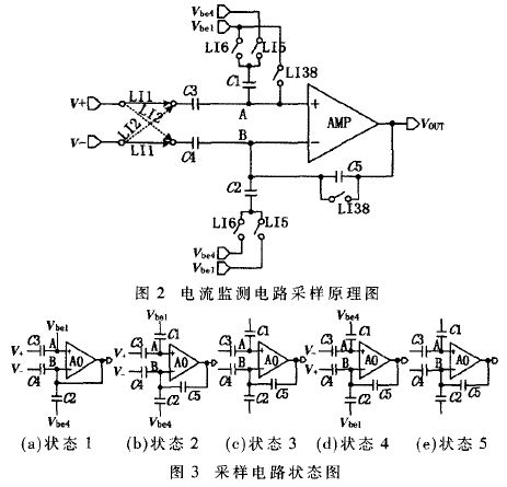
(1) LIl, LI2, LI38, LI5, LI6=10101, VA=Vbe1, VB=Vbe1, VC1=0, VC2=Vbe1 - Vbe4, VC3=Vbe1 - V+, VC4=Vbe1 - V-, VC5=0, VOUT is:
VOUT = VB = Vbe1 (1)
(2) LI1, LI2, LI38, LI5, LI6=10001, state 2 remains state 1 after switch switching, then VOUT = Vbe1.
(3) LI1, LI2, LI38, LI5, LI=00000, the switch is completely disconnected, and the previous state is maintained, VOUT = Vbe1.
(4) LI1, LI2, LI38, LI5, LI6=01010, V+, V-switch, Vbe1, Vbe4 also switch. According to the C1, C3 charge conservation law:
It is known from the characteristics of the op amp that VB = VA. It is known that VA and VB can obtain VC1 = VA - Vbe4, VC2 = VB - Vbe1, VC3 = VA - V-, VC4 = VB - V+, VC5 = VB - VOUT, according to the C2, C5 charge conservation law:
Wherein, the positive and negative of V--V+ are controlled by mutually non-overlapping clocks LI1, LI2. When LI1 is high in state l, V--V+ is positive; when LI1 is low in state 1, V--V+ is taken negative. The LI1 and LI2 switches are controlled at regular intervals, and the V+ and V- connections can be used to monitor the battery charge and discharge status in real time. According to equation (3) and Figure 1, VOUT and Vbe1 will produce a difference of ΔV by comparison with the comparator. At this time, changing the value of the sampling parallel capacitor n can adjust ΔV to quantify.
(5) LI1, LI2, LI38, LI5, LI6=00000, all switches are off, oUr remains in the previous state.
1.2 AMP amplifier circuit
AMP amplifier circuit shown in Figure 4, mainly includes: (1) self-bias circuit, composed of MPI3~MPI9, QPI1 and QPI4; (2) two-stage op amp, including MPI26, MPI27 full differential amplifier, MNI25 The source amplifier and Miller compensation consisting of MNI24 and CIl5. Among them, LI12 and LI17 are differential inputs; LI26 is the reset signal; H module is the digital power-on circuit; Vbe1 and Vbe4 are the reference outputs; LI22 is the operation output.
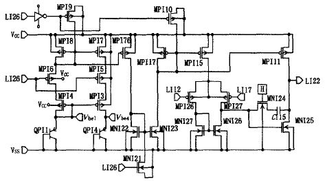
Figure 4 AMP amplifier circuit diagram
The self-bias circuit has an enable signal, and if the operation is abnormal, the circuit can be directly turned off. When LI26 is low, MPI9 is ​​turned off, MPI5 and MPI6 are turned on, the circuit works normally, and MPI4, MPI6 and MPI8 form the starting branch, then:
VCC≥2 VMPgs +Vbe (4)
Among them, VMPgs is the Vth of PMOS, and Vbe is the diode turn-on voltage. As long as VCC satisfies equation (4), the circuit can start normally. However, in the design, the influence of the shimming effect on the threshold should be considered, and the VCC is slightly higher than the calculated value. The QPI1 and QPI4 emitter area ratio is 1:4, so that the difference between Vbe1 and Vbe4 is VTln4. When LI26 is high, MPI9 is ​​turned on, MPI5 and MPI6 are turned off, and the circuit is turned off.
The AMP amplifier has Miller compensation, and the AC small signal equivalent circuit diagram is shown in Figure 5. Where gm1 and gm2 are the first and second level transconductances, respectively. The gain is expressed as:
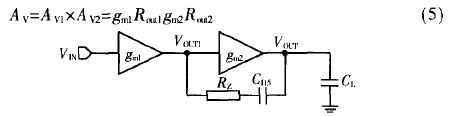
Figure 5 AMP amplifier AC small signal equivalent diagram
Wherein, Rout1 and Rout2 are output resistances of the first stage and the second stage, respectively, and Rout1 is a parallel connection of Rds_MPI27 and Rds_MNI26, Rout2 is a parallel connection of Rds_MPI11 and Rds_MNI25, and C1 is an equivalent load capacitance. In order to stabilize the system, the poles of the entire loop need to be analyzed:
Among them, CI15 is Miller capacitance, C1 is VOUT1. Node equivalent capacitance, Rz is MNI24 equivalent resistance (ie zero resistance). It can be seen from equation (9) that adjusting the Rz and CI15 can achieve system stability.
1.3 COMP high speed comparator circuit
As shown in Figure 6, the circuit consists of MN1~MN6 and MP1~MP4. IN1 and IN2 are the input terminals; OUT1 and OUT2 are the output terminals; LG99 is controlled by the digital clock to implement the reset function.
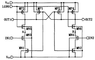
Figure 6 COMP high speed comparator circuit
The circuit uses positive feedback technology and the speed is greatly improved. When LG99 is low, MP3 and MP4 are turned on, MN5 and MN6 are turned off, OUT1 and OUT2 are raised, and the back-end flip-flop is in the hold state. When LG99 is high, MP3 and MP4 are turned off, and MN5 and MN6 are turned on. At this time, if IN1 is greater than IN2, V decreases and OUT1 decreases; OUT1 acts on MP2 and MN2, causing OUT2 to be raised; and OUT2 acts on MP1 and MN1, causing OUT1 to be pulled low to form positive feedback. Vice versa, as long as there is a voltage difference between IN1 and IN2, it will respond quickly on the output.
2 Simulation results and analysis
In this paper, the digital clock, AMP operational amplifier, bias circuit and high-speed comparator are simulated by H-spice in 0.18μm CMOS process.
Figure 7 shows the AC small-signal simulation data of the AMP amplifier, in which the reset signal LI26 is low, and an AC small signal of AC=1 is added to the LI12. AC scanning at -40 ° C, 25 ° C, 125 ° C three temperatures, we can see: (1) when the gain is reduced to 0, the phase margin remains above 90 degrees; (2) at different temperatures, gain and phase margin The degree is not affected and the system is in a stable state.
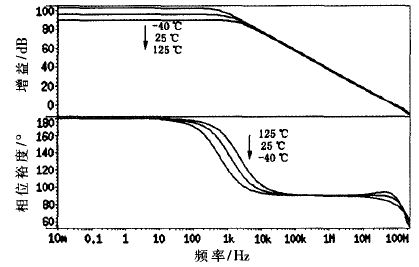
Figure 7 Amplifier gain and phase margin curves at different temperatures
Figure 8 shows the static operating point simulation data of the COMP high-speed comparator. LG99 is the reset signal, IN1 is 1.200 V, and transient scanning is performed on IN2 in the range of 1.200 V~1.210 V. If IN1=IN2, the output should be higher than the digital trigger level to ensure the timing is correct. After simulation, it can be known that: (1) there is an offset voltage in the circuit. When IN2 increases, a small amount of output does not match the digital logic. (2) When the input is equal, the output static working point is 1.5 V, which can ensure the back-end flip-flop remains; (3) The input can be set high or low quickly by inputting a difference of no more than 5 mV.
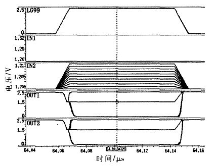
Figure 8 High-speed comparator static operating point simulation curve
Figure 9 shows the sampling data of the sampling circuit. SRP and SRN are the current sampling terminals of the lithium battery. The typical difference range is -125 mV~125 mV. LI22 is the output of the op amp. The input difference changes from 125mV to 5mV and then jumps to -125mV. The output corresponding to the voltage change at the sampling end is quantized according to the magnitude of the signal, and the output is judged to be in the charging or discharging state. However, the switch feedthrough effect may occur at the moment of switching, and the circuit increases the parasitic capacitance of the input of the op amp, effectively reducing the influence of frequent switching switches on the output.
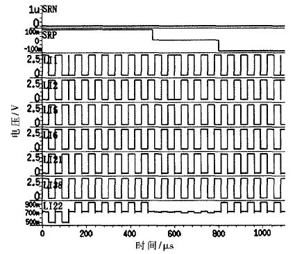
Figure 9 sampling circuit simulation curve
The overall simulation of the sampling circuit is not complete. When the difference between SRP and SRN changes in real time, the ability of the sampling circuit to follow the change is shown in Figure 10. The voltage of the fixed SRN is 0V, and a sine wave signal is added to the SRP for scanning. It can be seen from the figure that the output of the amplifier changes according to the change of the SRP, and the resolution of the sampling can meet the requirements.
This paper designs a current monitoring circuit for lithium batteries, which can accurately monitor current and charge and discharge status. This information can be used to control the activation of the protection circuit and can be used to accurately calculate parameters such as battery impedance and power. The circuit adds an enable control that shuts down the circuit when it is abnormal. And the offset setting can adjust the aspect ratio of MPI3, MPI4, MPI7, MPI8 tube (as shown in Figure 4), thereby achieving lower power consumption and improving battery life.
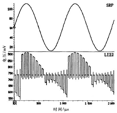
Figure 10 sampling circuit follow function simulation curve
1, Simple And Easy To Use App - Download our App Via Apple Store Or Google Play, You Can Track And Manage Your Health Index At Any Time.
2, Essential Body Composition Analysis - Body Weight Scale Not Only Display Weight, But Also View More Data On The App Including Bmi, Bmr,Body Fat %, Water %, Skeletal Muscle, Fat-Free Body Weight, Visceral Fat, Muscle Mass,Protein, Etc,It Will Keep You Informed About Your Body Data.
3, High Precision And Automatic Calibration - 4 High Precision Sensorsan Measure In Increments Of 0.2 Lb./0.1 Kg With 396Lbs/180Kg Capacity.
4, Enjoy Step-On Technology And Auto-Calibration,Just Step On The Smart Weight Scale To Get Timely Readings.
Bathroom Weight Scale,Digital Bathroom Scale,Accurate Bathroom Scale,Digital Weighing Scale Price
Axiswell Technology Co., Ltd , https://www.medhealthycare.com