Design and implementation of high-speed USB interface in IR-UWB communication system
Abstract: A high-speed USB interface is used to connect the computer terminal and the UWB communication system baseband module. A USB interface circuit is designed and implemented to control the data transmission between the UWB communication system baseband module and the USB interface device. Finally, the data transmission between the terminal computer and the UWB communication system is realized. . In the actual test, the speed of the USB interface is about 300 MB / s, which meets the high-speed transmission requirements stipulated by the USB 2.0 specification.
Keywords: UWB communication system; USB interface; USB interface circuit
IR-UWB (Ultra Wide Band Impulse Radio) wireless communication is a method that does not use a carrier, but uses pulses with extremely short time intervals for communication. It is also called impulse radio (Impulse Radio) and carrier-free (CarTIer Free) communication. In April 2001, China issued the "Tenth Five-Year Plan" 863 plan, which listed key UWB wireless communication technologies and coexistence and compatibility technologies as the main research projects of related communication technologies. Many universities also made UWB research as a key scientific research project and achieved A lot of progress. Among them, the UWB communication demonstration system involved in the research and development of a university requires that streaming media can be transmitted within a distance of 10 m. Based on this UWB communication demonstration system, the interface requirements of the UWB communication system and the terminal equipment are analyzed, and the high-speed USB interface is selected. The scheme uses FPGA technology to realize the data transmission of USB interface hardware control circuit, computer terminal and UWB communication system baseband module.
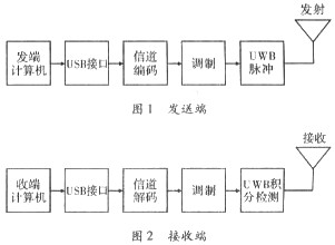
1 High-speed IR-UWB communication system program and implementation As shown in Figure 1, Figure 2. The IR-UWB communication system consists of a computer-side source sink, UWB transmitter, UWB receiver, baseband signal processing, and ultra-wideband transceiver antenna. In this system, the center frequency of the transmitted signal reaches 3.5 GHz, the UWB pulse envelope width is between 4 and 6 ns, the spectral bandwidth is not less than 500 MHz, the indoor transmission distance is within 10 m, and the transmitted signal spectrum meets the FCC spectrum template It is required that the channel transmission rate can reach 100 MB · S-1.
1.1 Baseband transmission scheme The baseband part is the key module of UWB communication equipment. It mainly completes the channel codec, the connection between the terminal and the communication system, as shown in Figure 3.
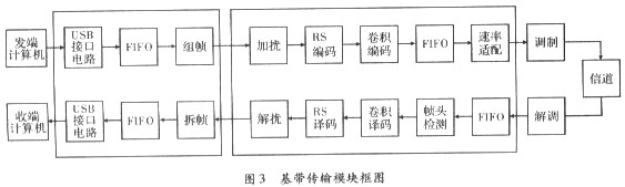
The UWB communication system has been implemented. The sender of the communication system uses a built-in source, and the receiver observes whether the data meets the index requirements through an oscilloscope. Obviously, such a method cannot reflect the performance of the UWB communication system, so the terminal interface must be expanded for the communication system. The high-speed USB interface is discussed in the article. USB is a new type of interface technology used in the computer field. It was first proposed by Compaq, Intel, Microsoft and other companies in November 1994. Its purpose is to use USB to replace the existing peripheral interfaces of PCs. The designed connection has the characteristics of simplification, plug and play, hot plug and so on. In order to support the transmission rate of 100 MB / s in the UWB communication system and ensure the real-time and smooth transmission of streaming media, the high-speed USB device is finally selected as the expansion interface of the communication system. The USB2.0 interface device is connected to the computer through a USB data line, and is connected to the communication system through an 8-bit data line. At the sending end, the function of the USB2.0 interface device is to collect the data sent by the computer and forward it to the baseband module of the UWB communication system; at the receiving end, the UWB receiver processes the received data through baseband processing and then through USB2.0 The interface device is forwarded to the computer.
1. 2 USB interface chip analysis and selection In this paper, EZ-USB FX2 series chip is selected as the USB interface chip, and the USB interface circuit is designed. The circuit controls the data transmission between the USB chip and the baseband module of the UWB communication system, and realizes the interconnection between the computer and the UWB communication system.
The USB2.0 protocol stipulates that the USB chip supports three transfer rates, namely 1.5 MB · s-1 low-speed transmission, 12 MB · s-1 full-speed transmission, and 480 MB · s-1 high-speed transmission. There are generally three commonly used USB function device interface chips: low-speed transmission chip CY7C630 / 1xxA, full-speed transmission chip EZ-USB series and high-speed transmission chip EZ-USB FX2 series. In order to support the transmission rate of up to 100 MB · s-1 of the UWB communication system, and to ensure the real-time and smoothness of streaming media transmission, the system selects the high-speed transmission series chip CY7C68013 as the USB interface chip.
2 Realization of the interface between the originating computer and the UWB communication system
2.1 USB interface scheme of the sending end As shown in Figure 4, the data transmitted by the computer of the control circuit transceiver end is stored in the 512-bit FIFO inside the USB chip, and a status signal u_flagc indicating that the FIFO is empty or not is generated at the same time. When u_flagc is high, the FIFO is not empty, otherwise it is empty. The 1 kBFIFO module is used for data buffering, and at the same time generates a flag signal that is full of wrfull and a signal usedw indicating how many bits of data in the FIFO are unread. The state detection and control module of the USB sending end is used to detect the flag signal of the corresponding state to generate the signal u_slrd for asynchronously reading the data in the USB interface FIFO. At the rising edge of u_slrd, the l bit in the USB interface FIFO is read out and the data Write to l kBFIFO. The data packing module packs the data according to the frame format.
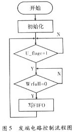
If u_flagc = 1 means there is data in the USB device. The FPGA control circuit reads data from the USB chip, and then judges whether the buffer of the FPGA control circuit still has space. If the buffer is not full, the data read from the USB chip is written into the FPGA buffer. In actual debugging, it is found that wrfull is at a high level, because in the effective time period, the rate of reading data is faster than that of writing.
2.3 Data framing module Complete the function of framing data and sending short packets. When the data in the 1 kB FIFO has 512 bits, the data is packaged and sent, that is, the header data E25F35 is sent first, then the data representing the frame length is sent, and finally the 512 bit frame data is sent. When the last frame of the transmitted file is less than 512 bits, the short packet sending function is used. First pack the remaining data, first send the frame header data, then send the remaining data size, and finally send the remaining data.
The data stream is transmitted in units of frames on the physical layer, so the data must be framed before being sent to the physical layer. Data frame structure, as shown in Figure 7.
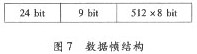
24 bit represents the header of this packet, and its value is E25F35. 9 bit represents the number of valid data bits in this packet. 512 × 8 bit represents 512 bit data, and the number of valid data is identified by 9 bits in front of the packet header. Only after detecting the header E25F35, the receiving end will process the 9 bits in front of the header and the 512 × 8 bits behind the header.
The flow of framing is shown in Figure 6. usedw indicates the number of bits of unread data stored in the 1 kB FIFO. If usedw≥512, there are 512 data in the 1 kB FIFO in Table 1 that can be packed into a complete package. If usedw <512 indicates that the data in the cache is less than one frame, then judge whether there is still data in the 1 kB FIFO. If usedw> 0, it means there is still data in the FIFO. TImer_count is a special counter that indicates how many consecutive clock cycles the data has not been read from the USB. When the data is read from the USB, it will be cleared. If TIme_count = 1 024lBai 0 means that no data has been read from the USB for 1024 clock cycles, the remaining data in the 1 kB FIFO is packed and sent with zero padding.
2. Realization of OSB interface circuit of sending end USB interface circuit of sending end, as shown in Fig. 8.
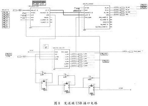
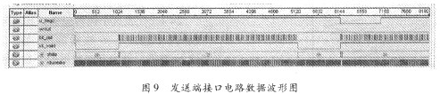
2.5 Data Waveform of the Interface Circuit at the Sending End Figure 9 is the Quartusâ…¡6 using FPGA development tool. O provides the logic analysis test chart of the virtual logic analyzer. As shown in Figure 9, u_flagc is the empty signal of the FIFO in the USB chip. It indicates whether there is data in the USB FIFO. If u_flagc is high, there is data. bit_out is the bit stream output after framing the data, and the bit stream will be sent to the baseband part of the communication system for channel coding. bit_valid is the high level corresponding to the valid data in bit_out. rdusedw represents the remaining data in the FPGA control circuit FIFO. When the data in the FPGA control circuit FIFO is full of 512 bits, the control circuit reads a frame of data from FIF0. state indicates the state transition of the state machine, 0 indicates the waiting state, the frame header data is sent in state 1, the frame length data is sent in state 2, and the valid data is sent in state 3.
3 Realization of interface between receiving computer and UWB communication system
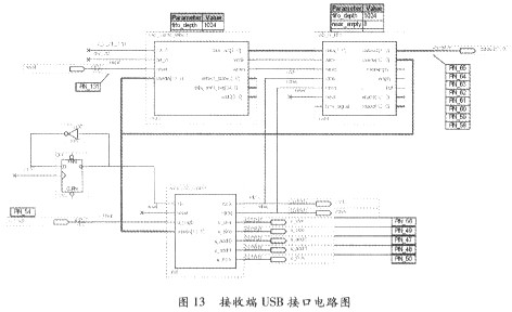
3.1 USB interface scheme at the receiving end As shown in Figure 10, the data deframing module preliminary buffers the bit stream data through the serial shift register, and simultaneously detects the data frame header. Once the frame header is detected, there is storage in the FIFO Space, deframe the buffered bit stream, and send the deframed data to the 128 kB FIFO, otherwise the frame header will always be detected. The 128 kB FIFO module is used for data buffering to match the rate between the modules before and after. The state detection and control module of the USB receiving end is used to detect the flag signal of the corresponding state, and generates the signals u_ifclk and u_slwr that are synchronously written to the data in the USB interface FIFO. The data on the bus is written into the USB interface chip.

3.2 The control circuit of the USB interface chip at the receiving end is shown in Figure 11.
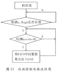
If the USB read request signal is detected, the state of the RAM is detected, and if there is data, the data is sent to the USB. When u_flagb is high, it means that the USB chip can receive data, otherwise it cannot receive data. Usedw> 0 means that there is data available in 128 kB FIFO, Usedw = 0 means that 128 kB FIF0 has no data available. At this time, the control signal to write data to the USB chip is in an invalid state.
3.3 The process of detecting the frame header and storing data in the FIFO is shown in Figure 12. First, the received data is buffered through a 35-bit deep shift register, and the frame header is detected in the buffered bit stream. Once the frame header is detected, the frame length data is taken out. At this time, whether the 128 kB FIFO has storage space is detected. If there is room, store and receive a frame of data, otherwise discard the frame data and re-detect the frame header. If "E25F35" is detected in the input bit stream, it is regarded as a frame header flag, and valid data of a total of 512 bits thereafter is written into RAM. If the frame header flag "E25F35" appears again in the valid data, the frame header judgment is not performed.
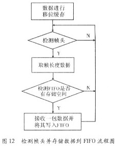
The conditions for writing data to the 128 kB FIFO are:
(1) Frame synchronization, that is, valid header data E25F35 can be detected;
(2) If frame_length represents frame length data, fifo_depth represents the data depth that FIF0 can accommodate. The 128 kB FIFO has the remaining space of frame_length to accommodate the data, otherwise the frame data is lost.
The detection condition is usedw + frame_length
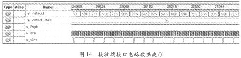
3.5 Data Waveform of Receiver Interface Circuit Figure 14 is a screenshot of the logic analysis test using the virtual logic analyzer provided by FPGA development tool Quartus II 6.0. As shown in Figure 14, dataout is the audio and video data output by the baseband module to the bus, and detect_state represents the frame detection state. 0 means waiting for detection, jump from 0 to 1 means to enter the frame detection state, jump from 1 to 2 means to enter the frame synchronization state, jump from 2 to 3 means to detect the data, and write the data to the FIFO in. u_flagb indicates that the FIFO in the USB chip is full, and u_flagb is high, indicating that data can be written to the USB chip. If u_flagb is low, it means that the USB chip FIFO is full and no more data can be written. u_ifelk is a synchronous write clock signal, u_slwr is a control write signal, and when u_slwr is low, write dataout to the USB chip.
1. Buy power banks from qualified factory,do not focus on cheap price
only. Batteries, circuit boards have certain fixed costs, higher quality
batteries, the higher purchase cost.
2. Better choose poly-mer
batteries. Polymer batteries output efficiency is relatively stable, but
also has a light weight, safe and efficient.
3. Consider shell beauty at the same time, pay attention to the shell strength and heat resistance.
4. Do not just focus on the conversion rate.
Lithium Polymer Battery Power Bank
Lithium Polymer Power Bank,10000Mah Power Bank,Lithium Polymer Battery Power Bank,4000Mah Power Bank
Custom Usb Gift company limited , https://www.customusbgift.com