In particular, Shanghai's motor companies completed all the first batches of reported data within a short period of more than 20 hours after the subsidy policy was announced. It is understood that more than a dozen motor companies such as Shanghai, Zhejiang, Jiangsu, and Fujian have been officially reported after the preliminary review.
On June 8th, Shanghai Electric Industry Association issued a notice to various related companies at the first time after obtaining information. At the same time, the Shanghai Municipal Development and Reform Commission issued a "Notice on Accelerating the Catalogue of Promotion of High-efficiency Motors for Motor Products Huimin Engineering" to all motor manufacturers.
On June 10, entrusted by the Shanghai Municipal Development and Reform Commission, a working meeting for the implementation of specific applications for the participation of more than 10 motor companies was held at the Municipal Energy Conservation Office. The complete set of submission materials was required to be reported promptly before 12 noon on the next day. Relevant companies spurred on the trend, leaders personally led the game, picked up a night light, and submitted relevant information on time. Other provinces and municipalities, at almost the same time, submitted application materials to the NDRC of each province and city.
On June 11, relevant departments of Shanghai conducted a preliminary review of the first batch of submitted companies and added relevant materials. It is understood that the state will announce the first batch of high efficiency motor Huimin project implementation units.
Multilayer PCB consist of 3 or more circuit layers bonded together by a thickness of insulating material called prepreg and core. They came into the industry with the advent of SMD population. They are found almost everywhere, wherever electronics are in use – from aircraft to motorcycles, and storage power stations to photovoltaics.
Multilayer PCBs are most complicated than others, and are generally considered to be the most sophisticated PCB product due to their construction methods and design complexities.
BentePCB offers multilayer printed circuit boards with the following special technologies:
· Edge plating for shielding and ground connection
· High frequency base materials for applications up to 80 GHz
· Cavities, countersunk holes or depth milling
· Thick copper up to 105μm (inner and outer layers)
· 500μm thick copper inlays using HSMtec technology
· Solder resist in green, white, black, blue, grey, brown, etc.
· Controlled impedances (single, differential, etc.)
· All recognised Printed Circuit Board industry surfaces available
|
Items |
Manufacturing Capabilities |
|
Number of Layers |
1-16 layers |
|
Material |
FR-4 |
|
Maximum PCB Size(Dimension) |
650x1200 mm |
|
Board Size Tolerance(Outline) |
±0.2mm/±0.5mm |
|
Board Thickness |
0.6-3.0mm |
|
Board Thickness Tolerance(t≥1.0mm) |
±10% |
|
Board Thickness Tolerance(t<1.0mm) |
±0.1mm |
|
Min Trace |
0.1mm/4mil |
|
Min Spacing |
|
|
Outer Layer Copper Thickness |
1oz/2oz/3oz/4oz(35μm/70μm/105μm/140μm) |
|
Inner Layer Copper Thickness |
1oz/2oz/3oz/4oz(35μm/70μm/105μm/140μm) |
|
Drill Sizes (CNC) |
0.2-6.3mm |
|
Min Width of Annular Ring |
0.15mm(6mil) |
|
Finished Hole Diameter (CNC) |
0.2mm-6.2mm |
|
Finished Hole Size Tolerance(CNC) |
±0.08mm |
|
Solder Mask |
LPI |
|
Minimum Character Width(Legend) |
0.15mm |
|
Minimum Character Height (Legend) |
0.8mm |
|
Character Width to Height Ratio (Legend) |
1:05 |
|
Minimum Diameter of Plated Half Holes |
0.6mm |
|
Surface Finishing |
HASL with lead |
|
HASL lead free |
|
|
Immersion gold |
|
|
Solder Mask |
Green ,Red, Yellow, Blue, White ,Black |
|
Silkscreen |
White, Black, None |
|
Panelization |
V-scoring, |
|
Tab-routing, |
|
|
Tab-routing with Perforation (Stamp Holes) |
About Us:
BentePCB is a professional PCB manufacturing which is focus on double side, multilayer, HDI PCB, rigid PCB and Flexible PCB mass production. The company was established on 2011.
We have two factories together, The factory in Shenzhen is specialized in small and middle volume orders and the factory in Jiangxi is for big volume.
Why Us?
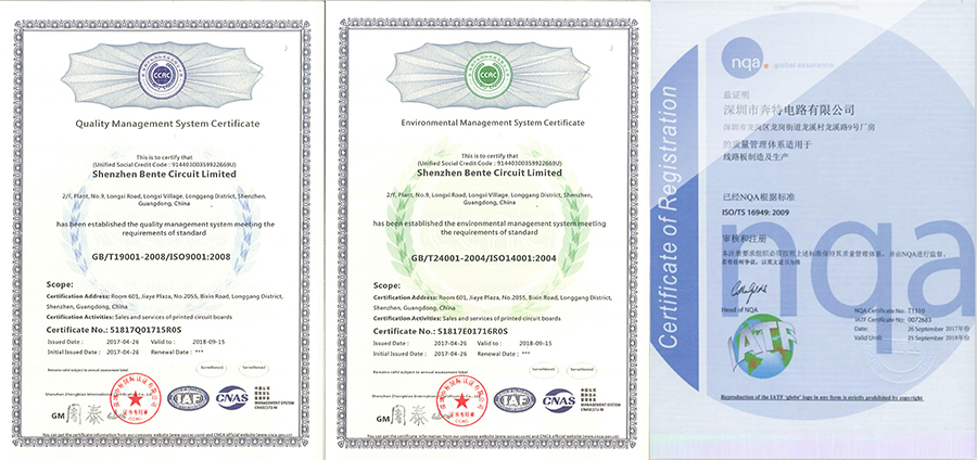
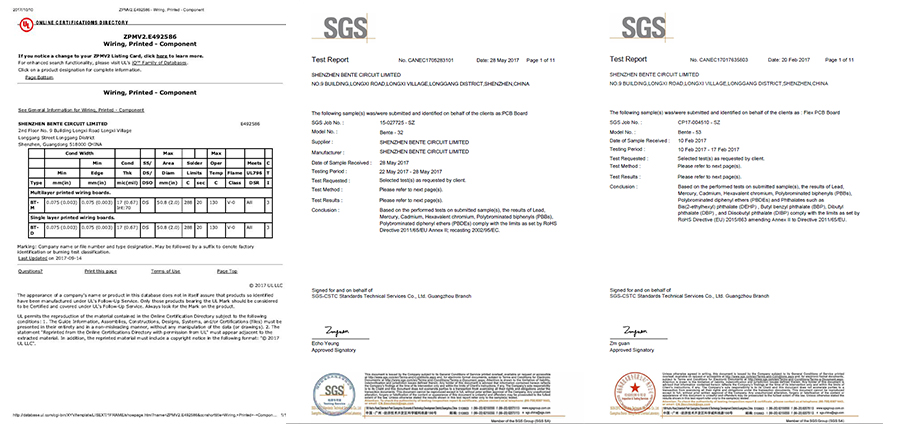
UL (E492586), ISO9001, ISO14001, TS16949, RoHS certified.
Turnover USD 10-50 million per year.
15,000 sqm area, 450 staff .
Mass Production from single to 16 layers.
Special Material:ROGERS, Arlon, Taconic.etc.
Client:Huawei, SAMSUNG, Malata, Midea,Texas Instruments.etc.
Certification(UL:E492586, TS16949, ISO14001, ISO9001,RoHS):
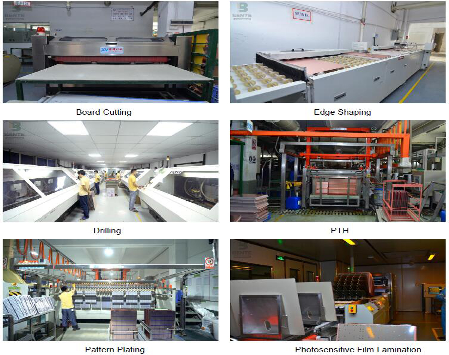
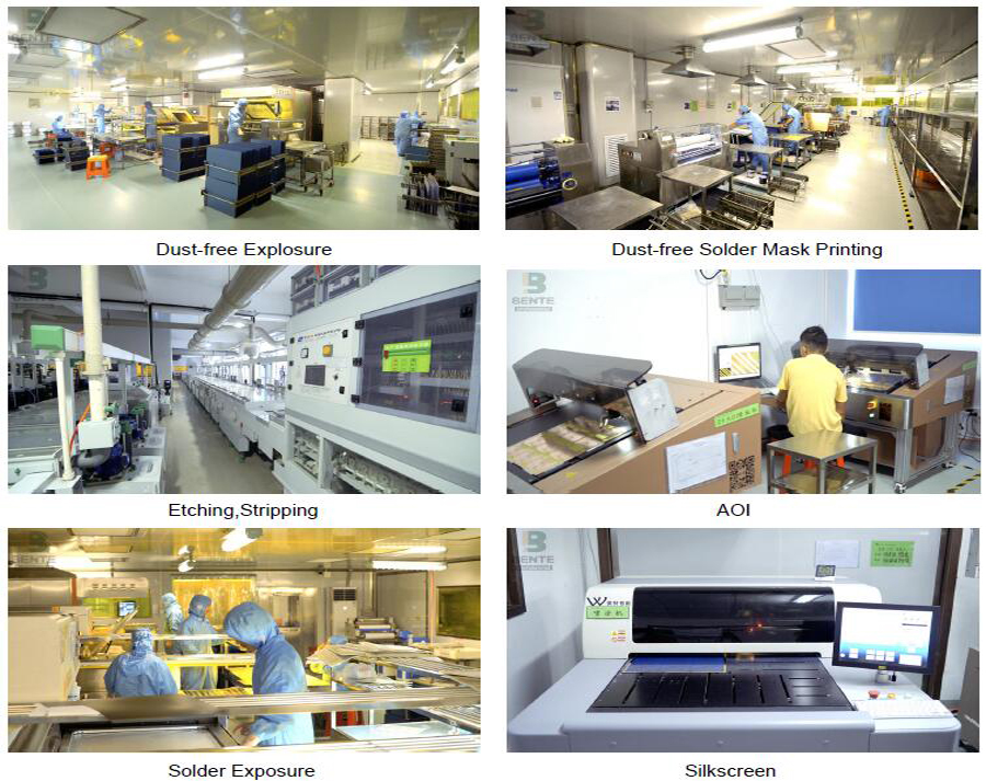
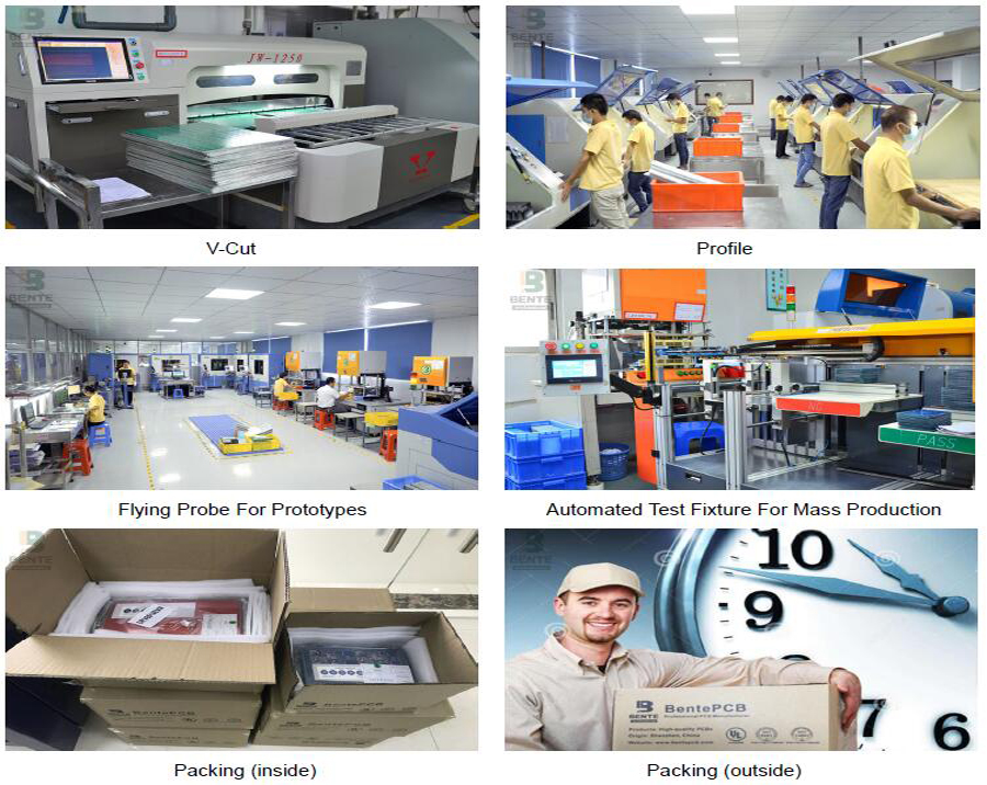
Factory Tour:
Exhibition:
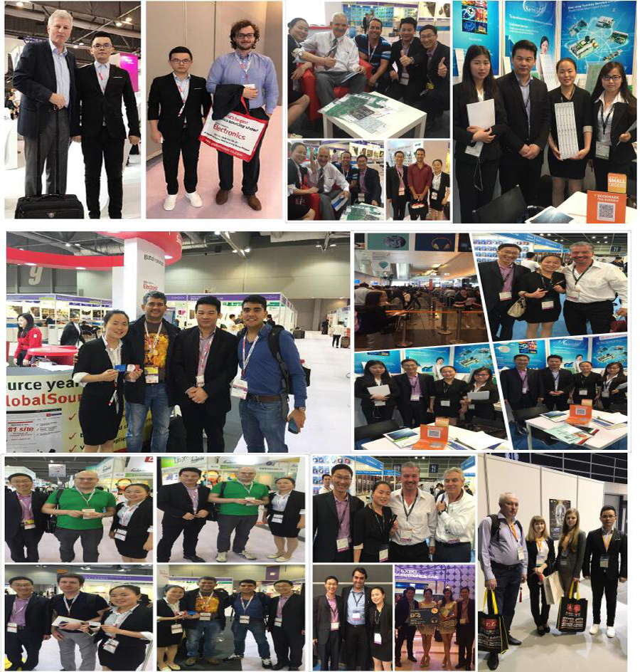
We Took part in the famous exhibitions over the past years,and got highly appreciation from the top experts,as well as cooperated tightly with them.
Delivery:
BentePCB offers flexible shipping methods for our customers, you may choose from one of the methods below.

FAQ:
Q1: What does BentePCB need for a customized PCB order?
A: The customers need to provide Gerber or pcb file.If you do not have the file in the correct format, you can send all the details related to the products.
Q2: What is your quotation policy?
A: For the PCB order in large quantity, BentePCB will send you the quotation based on the MOQ of the products concerned, and the price will be reasonable with good quality.
Q3: How long will you send us quotation ?
A: After all files were sent, 2 to 8 hours as per your file.
Q4: What is your minimum order quantity?
A:Our MOQ is 1 PCS.
Q5: How about the service BentePCB offered to the customers?
A: If you have any questions about our products or company, do not hesitate to send us your inquiry to our customer service representatives, Your satisfaction is our pursuits.


Multilayer PCB
Multilayer PCB, Multilayer PCB Design, Multilayer Circuit Board, Rigid Multilayer PCB
Shenzhen Bente Circuit Limited , http://www.bentegroup.com