1 Introduction
In the 1970s, CCD image sensors and CMOS image sensors started at the same time. Due to its high sensitivity and low noise, CCD image sensors have gradually become the mainstream of image sensors. However, due to process reasons, the sensitive components and signal processing circuits cannot be integrated on the same chip, resulting in a large volume and high power consumption of the camera assembled by the CCD image sensor. CMOS image sensors are unique in the image sensor market due to their small size and low power consumption. However, the CMOS image sensor on the market has not been free from the disadvantages of low light sensitivity and low image resolution, and the image quality cannot be compared with the CCD image sensor.
If the illumination sensitivity of the CMOS image sensor is further increased by 5 to 10 times, the noise is further reduced, and the image quality of the CMOS image sensor can reach or slightly exceed the level of the CCD image sensor while maintaining small size, light weight, and power consumption. Low, high integration, low price, etc., CMOS image sensor will become a reality instead of CCD image sensor.
Due to the application of CMOS image sensors, the development of a new generation of image systems has been greatly developed, and with the formation of economic scale, its production costs have also been reduced. The picture quality of CMOS image sensors is now comparable to that of CCD image sensors, thanks to improvements in image sensor chip design, and sub-micron and deep sub-micron designs that add new features inside the pixel.
In fact, more precisely, the CMOS image sensor should be an image system. A typical CMOS image sensor typically consists of: an image sensor core (which multiplexes discrete signal levels into a single output, much like a CCD image sensor), all timing logic, a single clock, and on-chip Programming features such as gain adjustment, integration time, window and analog to digital converter. In fact, when a designer purchased a CMOS image sensor, he got all the systems including image array logic registers, memory, timing pulse generators, and converters. Compared with the traditional CCD image system, integrating the entire image system on one chip not only reduces power consumption, but also has the advantages of light weight, reduced space consumption and lower overall price.
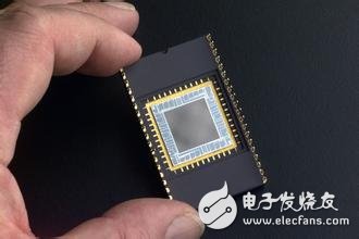
Figure 1 Early CCD image sensor
2, the basic principle
In one respect, CMOS image sensors have an amplifier in each pixel location, which allows them to convert discrete charge packets into voltage outputs at very low bandwidths, and only needs to be in frames. Reset at rate. One of the advantages of a CMOS image sensor is that it has a low bandwidth and increases the signal to noise ratio. Due to manufacturing process limitations, earlier CMOS image sensors were unable to place the amplifier within the pixel location. This technology, called PPS, is not ideal for noise performance, but it also introduces various interferences with CMOS image sensors.
Today, however, as the manufacturing process improves, the idea of ​​adding complex functions inside the pixel becomes possible. Now, within the pixel position, various additional functions such as electronic switches, transimpedance amplifiers, and related double-sample-and-hold circuits for reducing fixed pattern noise and noise cancellation have been added. In fact, on the CMOS image sensor used by an advanced CMOS camera from Conexant (formerly Rockwell Semiconductor), six transistors were designed and used in each pixel, and the read noise detected was only 1 rms. electronic. However, as the number of circuits in the pixel continues to increase, the space left for the photodiode is gradually reduced. In order to avoid this ratio (also known as the duty factor or the fill factor), microlenses are generally used because each pixel The tiny lens in the position changes the direction of the incident light, causing the light that would otherwise fall on the connection point or transistor to return to the diode area that is sensitive to light.
Another inherent advantage of CMOS image sensors is their anti-halation characteristics because the charge is limited to within the pixel. The voltage generated in the pixel position is first switched into a buffer of one column and then transferred to the output amplifier, so that the charge loss during transmission and the subsequent halo phenomenon do not occur. The disadvantage is that there is a small difference in the threshold voltage of the amplifier in each pixel, and this non-uniformity causes fixed image noise. However, with the continuous improvement of the structural design and manufacturing process of CMOS image sensors, this effect has been significantly weakened.
This versatile integration has made it possible for many previously unusable image technologies, such as children's toys, more dispersed security cameras, cameras embedded in monitors and laptop monitors, and cameras. Mobile circuits, fingerprint recognition systems, and even disposable cameras used in medical images have been considered by some designers.
3 design considerations
However, there is still a general concern in this industry, that is, measurement methods, lack of uniform standards for specific indicators, array size and characteristics. When comparing engineers to various data sheets, you may find that information on readout noise or signal-to-noise ratio is listed on one table, while on another table, it may only emphasize dynamic range or maximum. Information on potential well capacity. Therefore, this requires designers to be able to determine which parameters are most important to them and to make the best use of the multi-product CMOS image sensor family.
Some key performance parameters are of interest to any type of image sensor, including signal-to-noise ratio, dynamic range, noise (fixed pattern noise and readout noise), optical size, and voltage requirements. Important parameters that should be known and used for comparison are: maximum well capacity, readout noise under various operating conditions, quantum efficiency, and dark current. Other parameters such as signal-to-noise ratio are derived from those basic metrics.
For low-light-level applications like security cameras, readout noise and quantum effects are the most important. However, for medium- and high-illumination applications such as outdoor photography, the larger maximum well capacity is more important.
Dynamic range and signal-to-noise ratio are the parameters that are most easily misunderstood and misused. The dynamic range is the ratio of the maximum well capacity to the lowest readout noise. It is misleading because the readout noise is often not measured at typical operating speeds, and dark current shot noise is often not calculated. Inside. The signal-to-noise ratio is primarily determined by the brightness level of the incident light (in fact, in the case of very low brightness, the noise may be larger than the signal).
Therefore, the signal-to-noise ratio should take into account all noise sources. Some data lists often ignore shot noise, which is the main source of noise for medium and high signal levels. The SNRDARK is explained, in fact, it is no different from the dynamic range. Digital signal-to-noise ratio or digital dynamic range is another confusing concept that shows only one characteristic of an analog/digital (A/D) converter. Although this may be important, it does not accurately describe the quality of the image. At the same time, we should also clearly understand that when the image sensor has multiple adjustable analog gain settings, the resolution of the analog/digital converter does not limit the dynamic range of the image sensor.
The blurring of the concept of optical dimensions is due to traditional concepts. Using a light guide camera can only produce useful images in a partial range. Its calculations include the conversion of the unit of measure and the method of rounding up. Using the round-up method, the diagonal of the image sensor is divided by 16 in millimeters to obtain the optical size in inches. For example, the size of 0.97 cm is 1.27 cm instead of 0.85 cm. If you choose an image sensor with an optical size of 0.85 cm, it is likely that there will be reflections (shadows) on the corners of the image. This is because some data lists deceptively use the round-down approach. For example, the size of 0.97 cm is referred to as 0.85 cm for the simple reason that the price of the 0.85 cm optical size image sensor is much lower than the price of the 1.27 cm optical size image sensor, but this adversely affects system performance. Therefore, designers should try out various image sensors to get the desired performance.
A big advantage of a CMOS image sensor is that it requires only a single voltage to drive the entire device. However, designers should still carefully lay out the board driver chip. According to actual requirements, the digital voltage and the analog voltage are separated as much as possible to prevent crosstalk. Therefore, good board design, grounding and shielding are very important. Although this image sensor is a CMOS device and has a standard input/output (I/O) voltage, its actual input signal is quite small and sensitive to noise.
So far, a highly integrated single-chip CMOS image sensor has been designed. Designers strive to make versatile applications for image-related applications, including automatic gain control (AGC), automatic exposure control (AEC), auto-balance (AMB), gamma positive, background compensation, and automatic black level correction. All color matrix processing functions are integrated into the chip. The CMOS image sensor allows on-chip registers to program the camera over the I2C bus, with the advantages of wide dynamic range, anti-floating and virtually no smear.
UVC with Ozone: have a very powerful function, can remov bad smell, decomposing the harmful smalls, use for bed, sofa, carpet, basement, storage room, etc. no longer feel inexplicably itchy.
UV Germicidal Lamp,UV Light,Non Ozone UVC Disinfection Lamp,Disinfection UV Lamp,UV Sterilizer Box,UV Sterilizer Bag.
Shenzhen Waweis Technology Co., Ltd. , https://www.waweis.com