0 Preface
In recent years, switching power supplies have been rapidly developed with their advantages of high efficiency, small size, and good output stability. However, due to the high frequency, high di/dt and high dv/dt in the working process of the switching power supply, the electromagnetic interference problem is very prominent. The domestic 3G certification has replaced the CCIB and CCEE certification, making the switching power supply electromagnetic compatibility. The requirements are more detailed and rigorous. Nowadays, how to reduce or even eliminate the EMI problem of switching power supply has become a very important issue for global switching power supply designers and electromagnetic compatibility (EMC) designers. This article discusses the reasons for the formation of electromagnetic interference in switching power supplies and the commonly used EMI suppression methods.
1 Analysis of interference sources of switching power supplies
The most fundamental reason for the electromagnetic interference generated by switching power supplies is the high di/dt and high dv/dt generated during operation. The surge current and spike voltage generated by them form a source of interference. The large capacitor charging and discharging used in the power frequency rectification filtering, the voltage switching during high frequency operation of the switching tube, and the reverse recovery current of the output rectifying diode are all such interference sources. The voltage and current waveforms in the switching power supply are mostly periodic waves close to a rectangle, such as the driving waveform of the switching transistor and the MOSFET drain source waveform. For rectangular waves, the reciprocal of the period determines the fundamental frequency of the waveform; twice the reciprocal of the rising or falling time of the pulse edge determines the frequency value of the frequency component caused by these edges, typically in the MHz range, and its harmonics The frequency is even higher. These high frequency signals all interfere with the basic signal of the switching power supply, especially the signal of the control circuit.
The electromagnetic noise of the switching power supply can be divided into two categories from the noise source. One type is external noise, such as common mode and differential mode noise transmitted through the power grid, and interference from external electromagnetic radiation to the switching power supply control circuit. The other type is electromagnetic noise generated by the switching power supply itself, such as harmonics generated by current spikes of the switching tube and the rectifier tube and electromagnetic radiation interference.
As shown in Figure 1, the common mode and differential mode noise contained in the power grid interfere with the switching power supply. The switching power supply also generates electromagnetic interference to other equipments and loads of the power grid while receiving electromagnetic interference (return noise and output noise in the figure). And radiation interference). On the one hand, the EMI/EMC design of the switching power supply should prevent the switching power supply from causing interference to the power grid and nearby electronic equipment. On the other hand, it is necessary to strengthen the adaptability of the switching power supply itself to the electromagnetic disturbance environment. The following is a detailed analysis of the causes and ways of switching power supply noise.
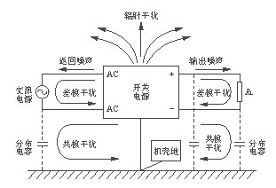
Figure 1 Switching power supply noise type diagram
1.1 Electromagnetic noise introduced by the power line
Power line noise is caused by electromagnetic disturbances generated by various electrical equipment in the power grid along the power line. Power line noise is divided into two categories: common mode interference and differential mode interference. Common-mode interference is defined as the undesired potential difference between any current-carrying conductor and the reference ground; differential-mode interference is defined as the undesirable between any two current-carrying conductors. Some potential differences. The equivalent circuit of the two kinds of interference is shown in Figure 2 [1]. In the figure, CP1 is the distributed capacitance between the primary and secondary of the transformer, and CP2 is the distributed capacitance between the switching power supply and the heat sink (ie, the distributed capacitance between the collector and the ground of the switching tube).
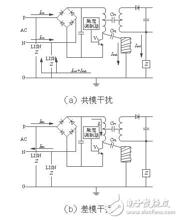
Figure 2 Equivalent circuit of two kinds of interference
As shown in Fig. 2(a), when the switching transistor V1 is turned off, the collector voltage suddenly rises to a high voltage. This voltage causes the common mode current Icm2 to charge the CP2 and the common mode current Icm1 to charge the CP1. The charging frequency of the distributed capacitor is the operating frequency of the switching power supply. Then the total common mode current in the line is (Icm1 + Icm2). As shown in Fig. 2(b), when V1 is turned on, the differential mode current Idm and the signal current IL flow along the circuit composed of the wire, the transformer primary, and the switching transistor. According to the equivalent model, the common mode interference current is transmitted through the input power line without passing through the ground. The differential mode interference current is transmitted through the ground and the input power line loop. Therefore, when we set the power line filter, we must consider the difference between differential mode interference and common mode interference, and use differential mode or common mode filter components to suppress their interference in the transmission path to achieve the best filtering effect.
1.2 Input noise caused by current distortion
The input of the switching power supply generally uses a bridge rectifier and a capacitor filter type rectified power supply. As shown in Fig. 3, in the input stage without PFC function, due to the nonlinearity of the rectifier diode and the energy storage of the filter capacitor, the conduction angle of the diode becomes small, and the input current i becomes a short time and a high peak. Periodic spike current. This distorted current contains a substantial amount of higher harmonic components in addition to the fundamental component. These higher harmonic components are injected into the grid, causing serious harmonic pollution and causing interference to other electrical appliances on the grid. In order to control the pollution of the switching power supply to the grid and achieve high power factor, the PFC circuit is an indispensable part.
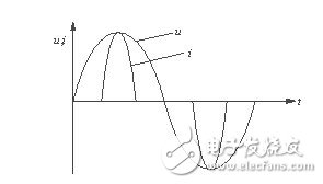
Figure 3 Input current and voltage waveform without PFC circuit
1.3 Disturbance caused by switch tubes and transformers
The main switch is the core component of the switching power supply and is also the source of interference. Its operating frequency is directly related to the intensity of electromagnetic interference. As the operating frequency of the switching tube increases, the switching speed of the switching tube voltage and current increases, and the conducted interference and radiation interference also increase. In addition, the reverse recovery characteristics of the anti-parallel clamp diodes on the main switch tube are not good, or the improper selection of the parameters of the voltage spike absorption circuit may also cause electromagnetic interference.
During the operation of the switching power supply, a high-frequency current loop is formed by the primary filter large capacitor, the high-frequency transformer primary coil and the switching tube. This loop produces large radiated noise. The load of the switching tube in the switching circuit is the primary coil of the high-frequency transformer, which is an inductive load. Therefore, spike noise occurs at the primary ends of the high-frequency transformer when the switching tube is turned on and off. The lighter causes interference, and the heavy one breaks through the switch tube. The distributed capacitance and leakage inductance between the main transformer windings are also important factors causing electromagnetic interference.
1.4 Output Rectifier Diode Interference
The ideal diode is turned off when subjected to a reverse voltage and no reverse current is passed. When the actual diode is conducting, the charge in the PN junction is accumulated. When the diode is subjected to the reverse voltage, the accumulated charge in the PN junction will be released and form a reverse recovery current, which will return to the zero point and junction capacitance. Related factors. The reverse recovery current will produce a strong high-frequency attenuation oscillation under the influence of transformer leakage inductance and other distributed parameters. Therefore, the reverse recovery noise of the output rectifier diode is also a major source of interference in the switching power supply. The RC buffer can be shunted across the diode to suppress its reverse recovery noise.
1.5 Distribution and parasitic parameters caused by switching power supply noise
The distributed parameter of the switching power supply is the internal factor of most interference. The distributed capacitance between the switching power supply and the heat sink, the distributed capacitance between the primary and secondary of the transformer, and the leakage inductance of the primary and secondary sides are all noise sources. Common mode interference is transmitted through the distributed capacitance between the primary and secondary of the transformer and the distributed capacitance between the switching power supply and the heat sink. The distributed capacitance of the transformer winding is related to the structure and manufacturing process of the high-frequency transformer winding. The distributed capacitance between the windings can be reduced by improving the winding process and structure, increasing the insulation between the windings, and using Faraday shielding. The distributed capacitance between the switching power supply and the heat sink is related to the structure of the switch tube and the way the switch tube is installed. The use of shielded insulating gaskets reduces the distributed capacitance between the switch and the heat sink.
As shown in Figure 4, the components under high frequency operation have high frequency parasitic characteristics [2], which affect their working state. When the high frequency is working, the wire becomes the emission line, the capacitance becomes the inductance, the inductance becomes the capacitance, and the resistance becomes the resonance circuit. Looking at the frequency characteristic curve in Fig. 4, it can be found that the frequency characteristics of the respective elements are considerably changed when the frequency is too high. In order to ensure the stability of the switching power supply during high-frequency operation, the design of the switching power supply should fully consider the characteristics of the component during high-frequency operation, and choose to use components with better high-frequency characteristics. In addition, at high frequencies, the inductive reactance of the parasitic inductance of the wire is significantly increased, and eventually becomes a single emission line due to the uncontrollability of the inductance. It has become a source of radiation interference in switching power supplies.
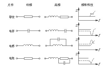
Figure 4 Frequency characteristics of components under high frequency operation
It is manufactured according to the GB4004-83.JB/T7600.3-94,DIN46395,it is made with the punched and compacted iron plate,and shaped with welding.With the big hardness and the lingt weight,it can fit for using in bunching,stranding,cabling,extrusion and the armouring machine.
|
d1
|
d2
|
d3
|
d4
|
d5
|
e
|
I1
|
I2
|
|
800
|
400
|
160
|
80
|
28-40
|
160
|
600
|
500
|
|
900
|
450
|
670
|
560
|
||||
|
1000
|
500
|
750
|
630
|
||||
|
1150
|
560
|
850
|
710
|
||||
|
1250
|
630
|
950
|
800
|
||||
|
1400
|
710
|
300
|
1060
|
900
|
|||
|
1600
|
800
|
1180
|
1000
|
||||
|
1800
|
1000
|
200
|
100
|
1320
|
1120
|
||
|
2000
|
1120
|
250
|
125
|
1500
|
1250
|
||
|
2240
|
1250
|
1700
|
1400
|
||||
|
2500
|
1500
|
1900
|
1600
|
||||
|
2800
|
1800
|
280
|
140
|
2120
|
1800
|
||
|
3150
|
1900
|
300
|
160
|
500
|
2300
|
2000
|

Enhanced Wire Spool, Large Spools For Wire, Welding Wire Spool, Barbed Wire Fence Spools
NINGBO BEILUN TIAOYUE MACHINE CO., LTD. , https://www.spool-manufacturer.com